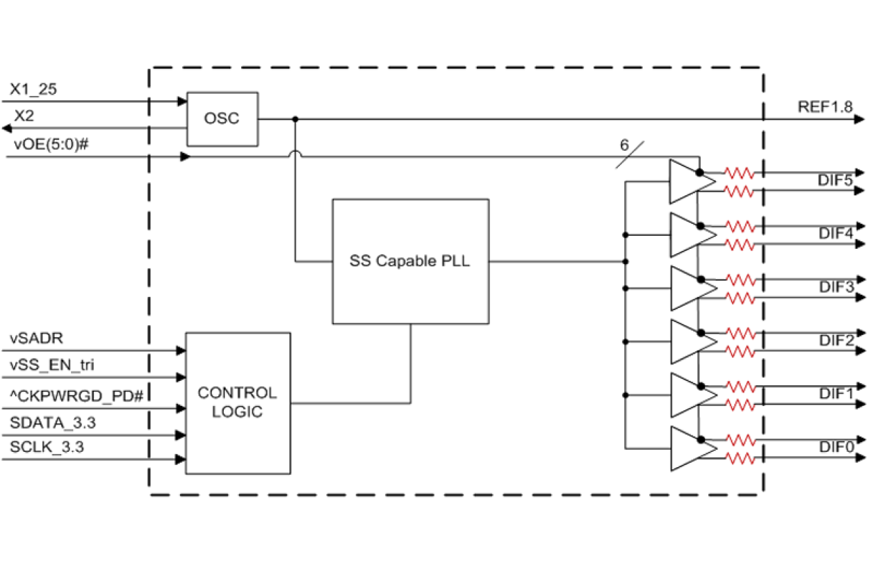
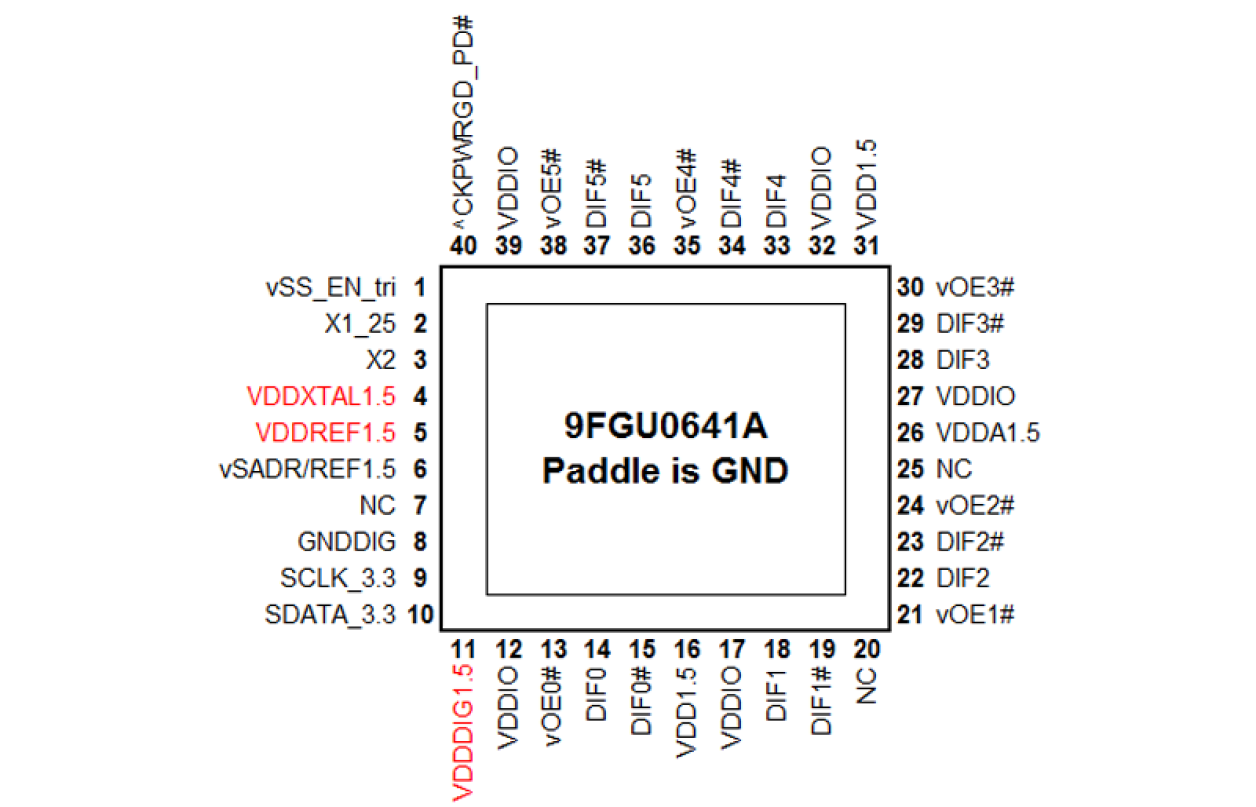
Features
- Direct connection to 100ohm transmission lines; saves 24 resistors compared to standard PCIe devices
- 45mW typical power consumption; reduced thermal concerns
- Outputs can optionally be supplied from any voltage between 1.05V and 1.5V; maximum power savings
- OE# pins; support DIF power management
- Programmable slew rate for each output; allows tuning for various line lengths
- Programmable output amplitude; allows tuning for various application environments
- DIF outputs blocked until PLL is locked; clean system start-up
- Selectable 0%, -0.25%, or -0.5% spread on DIF outputs; reduces EMI
- External 25MHz crystal; supports tight ppm with 0ppm synthesis error
- Configuration can be accomplished with strapping pins; SMBus interface is not required for device control
- 3.3V tolerant SMBus interface works with legacy controllers
- Space saving 6mm x 6mm 48-pin VFQFPN; minimal board space
- Selectable SMBus addresses; multiple devices can easily share an SMBus segment
Description
The 9FGU0641 is a member of Renesas' 1.5V ultra-low power PCIe clock family with integrated output terminations providing Zo = 100Ω. The device has six output enables for clock management and supports two different spread spectrum levels in addition to spread off.
For information regarding evaluation boards and material, contact your local sales representative.
Parameters
| Attributes | Value |
|---|---|
| Diff. Outputs | 6 |
| Diff. Output Signaling | LP-HCSL |
| Output Freq Range (MHz) | 25 - 25, 100 - 100 |
| Power Consumption Typ (mW) | 45 |
| Supply Voltage (V) | 1.5 - 1.5 |
| Output Type | LP-HCSL, LVCMOS |
| Xtal Freq (MHz) | 25 - 25 |
| Diff. Termination Resistors | 0 |
| Package Area (mm²) | 25 |
| Battery Backup | No |
| Battery Seal | No |
| CPU Supervisory Function POR | No |
| Crystal Frequency Trimming | No |
| Frequency Out Pin | No |
| Inputs (#) | 1 |
| Input Freq (MHz) | 25 - 25 |
| Function | Generator |
| Input Type | Crystal, LVCMOS |
| Core Voltage (V) | 1.5 |
| Output Voltage (V) | 0.8V, 1.5V |
| Product Category | PCI Express Clocks |
Package Options
| Pkg. Type | Pkg. Dimensions (mm) | Lead Count (#) | Pitch (mm) |
|---|---|---|---|
| VFQFPN | 5.0 x 5.0 x 0.9 | 40 | 0.4 |
Applied Filters:


