Overview
Description
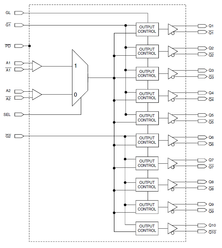
The 5T9310 is a low skew, 1-to-10 differential LVDS clock fanout buffer. The device has two selectable inputs. The inputs accept LVDS, HSTL, CML, LVPECL and single-ended signals such as 3.3V/2.5V LVCMOS/LVTTL. The 5T9310 outputs can be asynchronously enabled/disabled. When disabled, the outputs will drive to the value selected by the GL pin. Multiple power and grounds reduce noise.
Features
- Operating frequency range: 0-1000 MHz
- Output skew: <25ps (maximum)
- Duty cycle distortion: <125ps (maximum)
- Selectable inputs
- Hot insertable and over-voltage tolerant inputs
- 3.3V/2.5V LVTTL, HSTL, LVPECL, CML or LVDS input interface
- Power-down mode
- 2.5V voltage supply
- -40°C to 85°C ambient operating temperature
Comparison
Applications
Design & Development

Product Options
Applied Filters: