Features
- Extremely low operating and standby current consumption
- Low RMS Additive Phase jitter
- 1.8V power supply voltage
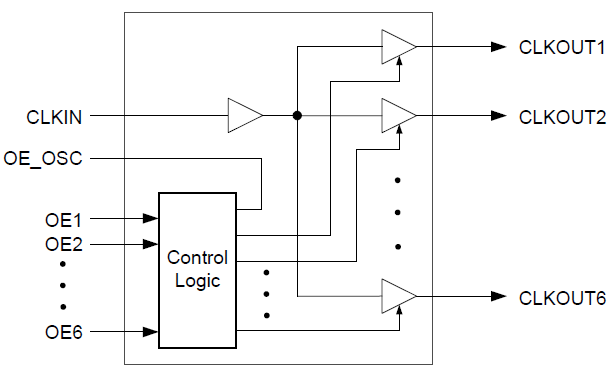
- Four outputs with individual Output Enable pin
- One input
- OE_OSC control pin to enable/disable reference TCXO / XO
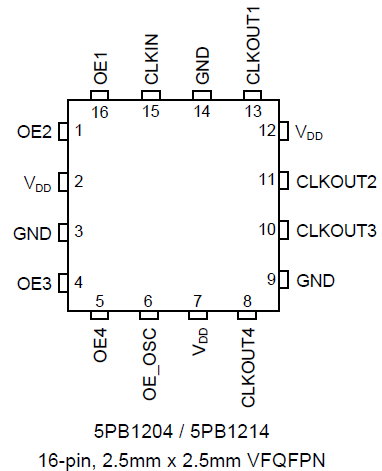
- Small 16-pin VFQFPN package
- Extended temperature range (-40 °C to +105 °C)
Description
The 5PB1204 is a high-performance TCXO/LVCMOS clock fanout buffer with individual OE pins for each output. The CLKIN pin can accept either a square wave (LVCMOS) or a clipped sine wave (such as TCXO clipped sine wave output) as input.
The 5PB1204 has industry-leading low jitter and extremely low current consumption, making it ideal for smart mobile devices.
Parameters
| Attributes | Value |
|---|---|
| Function | Buffer |
| Outputs (#) | 4 |
| Output Type | LVCMOS |
| Output Freq Range (MHz) | - |
| Input Type | LVCMOS, Sine Wave |
| Output Banks (#) | 1 |
| Output Voltage (V) | 1.8 |
| Output Skew (ps) | 65 |
| Additive Phase Jitter Typ RMS (fs) | 50 |
Package Options
| Pkg. Type | Pkg. Dimensions (mm) | Lead Count (#) | Pitch (mm) |
|---|---|---|---|
| COL | 2.5 x 2.5 x 0.5 | 16 | 0.4 |
Applications
- Smart mobile handsets
- RF and baseband peripheral clock distribution
- Automotive