概要
説明
Support is limited to customers who have already adopted these products.
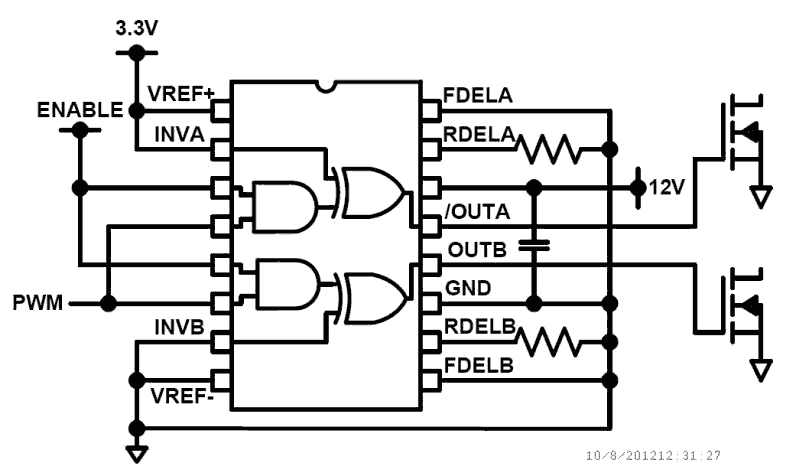
The ISL89367 is a high-speed, 6A, 2 channel MOSFET driver optimized for synchronous rectifier applications. Internal timers can be programmed with resistors to delay the rising and/or falling edges of the outputs. Logically ANDed dual inputs are also provided. One input is for the PWM signal and the second can be used as an enable. A third control input is used to optionally invert the logical polarity of the driver outputs. Comparator like logical inputs allows this driver to be configured for any logic level from 3. 3V to 10 VDC. The precision logic thresholds provided by the comparators allow the use of external RC circuits to generate longer time delays than are possible with the internal timers. The comparators also allow the driver to be configured with a low output voltage that is negative relative to the logic ground if desired. This is useful for applications that require a negative turn-off gate drive voltage for driving FETs with logic thresholds. At high switching frequencies, these MOSFET drivers use very little bias current. Separate, non-overlapping drive circuits are used to drive each CMOS output FET to prevent shoot-thru currents in the output stage. The start-up sequence is design to prevent unexpected glitches when VDD is being turned on or turned off. When VDD ~1V, an internal 10kΩ resistor between the output and ground helps to keep the output voltage low. When ~1V VDD UV, both outputs are driven low with very low resistance and the logic inputs are ignored. This insures that the driven FETs are off. When VDD > UVLO, and after a short delay, the outputs now respond to the logic inputs.
特長
- 2 outputs with 6A peak drive currents (sink and source) with output voltage range of 4.5V to 16V
- Typical ON-resistance <1Ω
- Specified Miller plateau drive currents
- EPAD provides very low thermal impedance (θJC = 3°C/W)
- Dual logic inputs with hysteresis for high noise immunity
- Rising and/or falling output edge delays programmed with resistors
- 20ns rise and fall time driving a 10nF load
- Flexible logic options available by use of INVA and INVB pins
製品比較
アプリケーション
ドキュメント
ピックアップ
ログイン後、ご登録が可能となります。
|
|
|
|
|---|---|---|
| 分類 | タイトル | 日時 |
| データシート | PDF 735 KB | |
| EOL通知 | PDF 200 KB | |
| 製品変更通知 | PDF 84 KB | |
| アプリケーションノート | PDF 509 KB | |
| アプリケーションノート | PDF 397 KB | |
| マニュアル-開発ツール | PDF 3.45 MB | |
| アプリケーションノート | PDF 576 KB | |
7件
|
||
設計・開発
モデル
ECADモデル
SamacSysの回路図シンボル、PCBフットプリント、および3D CADモデルは、製品オプションテーブルのCADモデルリンクをクリックすることで参照できます。シンボルまたはモデルが対応していない場合は、SamacSysに直接リクエスト可能です。

製品選択
適用されたフィルター


