パッケージ情報
| CADモデル: | View CAD Model |
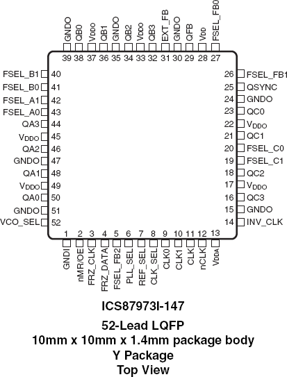
| Pkg. Type: | TQFP |
| Pkg. Code: | PPG52 |
| Lead Count (#): | 52 |
| Pkg. Dimensions (mm): | 10.0 x 10.0 x 1.4 |
| Pitch (mm): | 0.65 |
環境及び輸出分類情報
| Moisture Sensitivity Level (MSL) | 3 |
| Pb (Lead) Free | Yes |
| ECCN (US) | EAR99 |
| HTS (US) | 8542.39.0090 |
製品スペック
| Lead Count (#) | 52 |
| Carrier Type | Reel |
| Moisture Sensitivity Level (MSL) | 3 |
| Qty. per Reel (#) | 500 |
| Qty. per Carrier (#) | 0 |
| Pb (Lead) Free | Yes |
| Pb Free Category | e3 Sn |
| Temp. Range (°C) | -40 to 85°C |
| Advanced Features | Programmable Clock |
| C-C Jitter Max P-P (ps) | 55 |
| Core Voltage (V) | 3.3 |
| Feedback Input | No |
| Input Freq (MHz) | 120 |
| Input Type | HCSL, HSTL, LVCMOS, LVDS, LVPECL, SSTL |
| Inputs (#) | 3 |
| Length (mm) | 10 |
| MOQ | 500 |
| Output Banks (#) | 4 |
| Output Freq Range (MHz) | 10 - 150 |
| Output Skew (ps) | 200 |
| Output Type | LVCMOS |
| Output Voltage (V) | 3.3 |
| Outputs (#) | 13 |
| Package Area (mm²) | 100 |
| Pitch (mm) | 0.65 |
| Pkg. Dimensions (mm) | 10.0 x 10.0 x 1.4 |
| Pkg. Type | TQFP |
| Prog. Clock | Yes |
| Prog. Interface | Serial |
| Reel Size (in) | 13 |
| Requires Terms and Conditions | Does not require acceptance of Terms and Conditions |
| Tape & Reel | Yes |
| Thickness (mm) | 1.4 |
| Width (mm) | 10 |
| 掲載 | No |
87973I-147 に関するリソース
説明
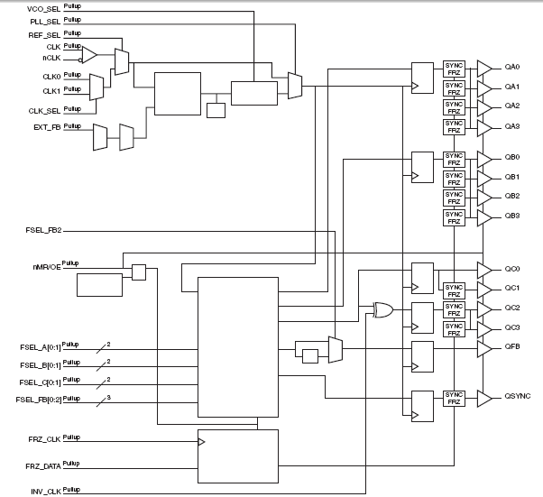
The 87973I-147 is a LVCMOS/LVTTL clock generator and a member of the HiPerClockS™ family of High Performance Clock Solutions from IDT. The 87973I-147 has three selectable inputs and provides 14 LVCMOS/LVTTL outputs. The 87973I-147 is a highly flexible device. The three selectable inputs (1 differential and 2 single ended inputs) are often used in systems requiring redundant clock sources. Up to three different output frequencies can be generated among the three output banks. The three output banks and feedback output each have their own output dividers which allows the device to generate a multitude of different bank frequency ratios and output-to-input frequency ratios. In addition, 2 outputs in Bank C (QC2, QC3) can be selected to be inverting or non-inverting. The output frequency range is 10MHz to 150MHz. The input frequency range is 6MHz to 120MHz. The 87973I-147 also has a QSYNC output which can be used for system synchronization purposes. It monitors Bank A and Bank C outputs and goes low one period prior to coincident rising edges of Bank A and Bank C clocks. QSYNC then goes high again when the coincident rising edges of Bank A and Bank C occur. This feature is used primarily in applications where Bank A and Bank C are running at different frequencies, and is particularly useful when they are running at non-integer multiples of one another.

