特長
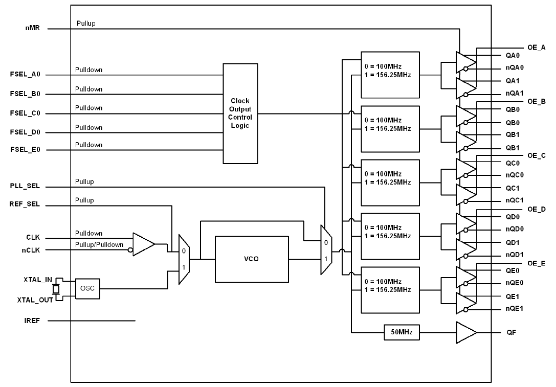
- Ten selectable 100MHz and 156.25MHz clocks for PCI Express,
sRIO and GbE, HCSL interface levels - One single-ended QF LVCMOS/LVTTL clock output at 50MHz, 15Ω output impedance
- Selectable external crystal or differential (single-ended) input source
- Crystal oscillator interface designed for 25MHz, parallel resonant crystal
- Differential CLK, nCLK input pair that can accept: LVPECL, LVDS, LVHSTL, and HCSL input levels
- Internal resistor bias on nCLK pin allows the user to drive CLK input with external single-ended (LVCMOS/ LVTTL) input levels
- PCI Express (2.5Gb/S), Gen 2 (5Gb/s) and Gen 3 (8Gb/s) jitter compliant
- Full 3.3V power supply
- -40 °C to 85 °C ambient operating temperature
- Lead-free (RoHS 6) packaging
説明
The 8413S12BI-126 is a PLL-based clock generator. This high-performance device is optimized to generate the processor core reference clock, the PCI Express, sRIO, XAUI, SerDes reference clocks, and the clocks for both the Gigabit Ethernet MAC and PHY. The clock generator offers ultra-low jitter, low-skew clock outputs. The output frequencies are generated from a 25MHz external input source or an external 25MHz parallel resonant crystal. The industrial temperature range of the 8413S12BI-126 supports telecommunication, networking, and storage requirements.
パラメータ
| 属性 | 値 |
|---|---|
| Outputs (#) | 11 |
| Output Type | LVCMOS, HCSL, LVTTL |
| Output Freq Range (MHz) | 100 - 100, 50 - 50, 156.25 - 156.25 |
| Input Freq (MHz) | 25 - 25 |
| Inputs (#) | 2 |
| Input Type | Crystal, LVCMOS, LVTTL, LVPECL, LVDS, LVHSTL, HCSL |
| Output Banks (#) | 7 |
| Core Voltage (V) | 3.3 |
| Output Voltage (V) | 3.3 |
パッケージオプション
| Pkg. Type | Pkg. Dimensions (mm) | Lead Count (#) | Pitch (mm) |
|---|---|---|---|
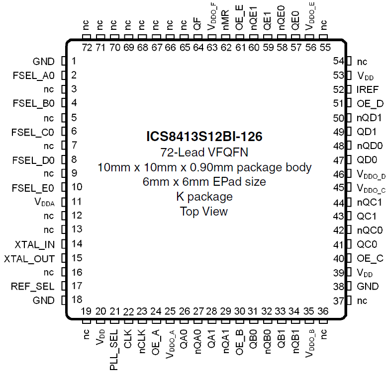
| VFQFPN | 10.0 x 10.0 x 1.0 | 72 | 0.5 |
アプリケーション
- CPE Gateway Design
- Home Media Servers
- 802.11n AP or Gateway
- Soho Secure Gateway
- Soho SME Gateway
- Wireless Soho and SME VPN Solutions
- Wired and Wireless Network Security
- Web Servers and Exchange Servers
適用されたフィルター
読込中


