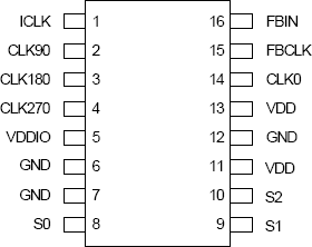
| Lead Count (#) | 16 |
| Pkg. Type | SOIC |
| Pkg. Code | DCG16 |
| Pitch (mm) | 1.27 |
| Pkg. Dimensions (mm) | 9.9 x 3.9 x 1.5 |
| Pb (Lead) Free | Yes |
| ECCN (US) | EAR99 |
| HTS (US) | 8542.39.0090 |
| Moisture Sensitivity Level (MSL) | 3 |
| Pkg. Type | SOIC |
| Lead Count (#) | 16 |
| Pb (Lead) Free | Yes |
| Carrier Type | Tube |
| Advanced Features | Feedback Input |
| C-C Jitter Typ P-P (ps) | 150 |
| Core Voltage (V) | 3.3, 5 |
| Feedback Input | Yes |
| Input Freq (MHz) | 5 - 150 |
| Input Type | LVCMOS |
| Inputs (#) | 1 |
| Length (mm) | 9.9 |
| MOQ | 144 |
| Moisture Sensitivity Level (MSL) | 3 |
| Output Banks (#) | 1 |
| Output Freq Range (MHz) | 15 - 84 |
| Output Skew (ps) | 300 |
| Output Type | LVCMOS |
| Output Voltage (V) | 3.3, 5 |
| Outputs (#) | 4 |
| Package Area (mm²) | 38.6 |
| Pb Free Category | e3 Sn |
| Period Jitter Typ P-P (ps) | 75.000 |
| Pitch (mm) | 1.27 |
| Pkg. Dimensions (mm) | 9.9 x 3.9 x 1.5 |
| Prog. Clock | No |
| Qty. per Carrier (#) | 48 |
| Qty. per Reel (#) | 0 |
| Requires Terms and Conditions | Does not require acceptance of Terms and Conditions |
| Tape & Reel | No |
| Temp. Range | 0 to 70°C |
| Thickness (mm) | 1.5 |
| Width (mm) | 3.9 |
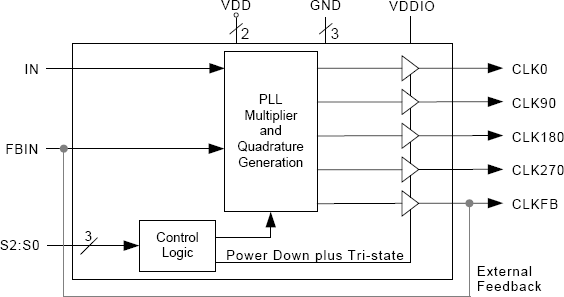
The 672-01/02 are zero delay buffers that generate four output clocks whose phases are spaced at 90° intervals. Based on IDT's proprietary low jitter Phase-Locked Loop (PLL) techniques, each device provides five low-skew outputs, with clock rates up to 84 MHz for the 672-01 and up to 135 MHz for the 672-02. By providing outputs delayed one quarter clock cycle, the device is useful for systems requiring early or late clocks. The 672-01/02 include multiplier selections of x0.5, x1, x2, x3, x4, x5, or x6. They also offer a mode to power-down all internal circuitry and tri-state the outputs. In normal operation, output clock FBCLK is tied to the FBIN pin. IDT manufactures the largest variety of clock generators and buffers, and is the largest clock supplier in the world.