概要
説明
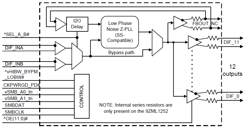
The 9ZML1252E is a second-generation 2-input/12-output differential mux for Intel Purley and newer platforms. It exceeds the demanding DB1200ZL performance specifications and is backward compatible with the 9ZML1232B. The device utilizes Low Power HCSL-compatible outputs to reduce power consumption and termination resistors. It is suitable for PCI Express Gen 1-4 or QPI/UPI applications, and provides two configurable low-drift I2O settings, one for each input channel, to allow I2O tuning for various topologies.
特長
- 2 configurable low-drift I2O delays up to 2.9ns; maintain transport delay for various topologies
- LP-HCSL outputs with Zout = 85Ω; eliminate 48 resistors
- 9 selectable SMBus addresses; multiple devices can share the same SMBus segment
- Separate VDDIO for outputs; allows maximum power savings
- PLL or Bypass Mode; PLL can de-jitter incoming clock
- Hardware or software-selectable PLL BW; minimizes jitter peaking in downstream PLLs
- Spread spectrum compatible; tracks spreading input clock for EMI reduction
- SMBus interface; software can modify device settings without hardware changes
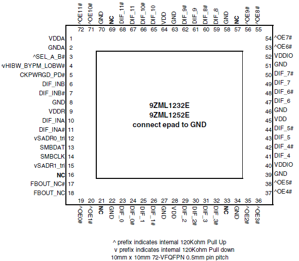
- 10mm x 10mm 72-QFN package; small board footprint
製品比較
アプリケーション
設計・開発
ボード&キット
Evaluation
EVK9ZXL1951D
アクティブ
Evaluation Kit for 19-Output DB1900Z for PCIe Gen1-4 and QPI/UPI
The evaluation board is designed to help the customer evaluate the 9ZXL1951D. The device is programmable through an SMBus interface. The user guide details the board set and connection, as well as the companion Graphical User Interface (GUI) installation for communicating with the device. The...
Recommended Documents:
モデル
ECADモデル
SamacSysの回路図シンボル、PCBフットプリント、および3D CADモデルは、製品オプションテーブルのCADモデルリンクをクリックすることで参照できます。シンボルまたはモデルが対応していない場合は、SamacSysに直接リクエスト可能です。

製品選択
適用されたフィルター
ビデオ&トレーニング
PCIe Gen5 Clock Buffers
Introducing Renesas’ enhanced PCIe clock buffer family. These PCIe Gen5 clock buffers offer fanout and zero-delay operating modes, supporting both legacy systems and the most complex timing trees within a single device. Unlike many existing solutions, whose performance limitations force their use in fanout buffer mode, these clock buffers meet both PCIe Gen5 and prominent CPU-specific phase jitter requirements in all operating modes. The extremely low 50fs rms PCIe Gen5 additive phase jitter enables multi-level cascading within the strict PCIe Gen5 jitter budget. Renesas’ high-performance oscillators and clock generators provide an ideal clock source for the enhanced PCIe clock buffer family.
For more information about these PCIe Gen5 clock buffers, visit the PCIe timing page.
Video List