| Lead Count (#) | 20 |
| Pkg. Type | VFQFPN |
| Pkg. Code | NDG20 |
| Pitch (mm) | 0.4 |
| Pkg. Dimensions (mm) | 3.0 x 3.0 x 0.9, 3.0 x 3.0 x 1.0 |
| Moisture Sensitivity Level (MSL) | 1 |
| Pb (Lead) Free | Yes |
| ECCN (US) | EAR99 |
| HTS (US) | 8542.39.0090 |
| Pkg. Type | VFQFPN |
| Lead Count (#) | 20 |
| Carrier Type | Tray |
| Moisture Sensitivity Level (MSL) | 1 |
| Qty. per Reel (#) | 0 |
| Qty. per Carrier (#) | 624 |
| Pb (Lead) Free | Yes |
| Pb Free Category | e3 Sn |
| Temp. Range | -40 to 105°C |
| Country of Assembly | Taiwan |
| Country of Wafer Fabrication | Singapore |
| Price (USD) | 1.91364 |
| Additive Jitter | 3.5fs |
| Additive Phase Jitter Typ RMS (fs) | 33 |
| Additive Phase Jitter Typ RMS (ps) | 0.033 |
| Advanced Features | Automatic Clock Parking, Flexible Power Sequencing and more... |
| App Jitter Compliance | PCIe Gen1, PCIe Gen2, PCIe Gen3, PCIe Gen4, PCIe Gen5, PCIe Gen6, PCIe Gen7 |
| Architecture | Common, SRIS, SRNS |
| Core Voltage (V) | 1.8, 1.8 |
| Diff. Inputs | 1 |
| Diff. Output Signaling | LP-HCSL |
| Diff. Outputs | 2 |
| Family Name | RC191 |
| Function | Multiplexer |
| Input Freq (MHz) | 1 - 400 |
| Input Type | LVDS, HCSL |
| Inputs (#) | 1 |
| Length (mm) | 3 |
| Longevity | 2040 Apr |
| MOQ | 624 |
| Output Banks (#) | 1 |
| Output Freq Range (MHz) | 1 - 400 |
| Output Impedance | 33, 85, 100 |
| Output Skew (ps) | 36 |
| Output Type | LP-HCSL |
| Output Voltage (V) | 0.8 |
| Outputs (#) | 2 |
| Pitch (mm) | 0.4 |
| Pkg. Dimensions (mm) | 3.0 x 3.0 x 1.0 |
| Power Consumption Typ (mW) | 50 |
| Prog. Interface | SMBus |
| Supply Voltage (V) | 1.8 - 1.8 |
| Tape & Reel | No |
| Thickness (mm) | 1 |
| VOUT Amplitude Control | Yes |
| VOUT Slew-rate Control | Yes |
| Width (mm) | 3 |
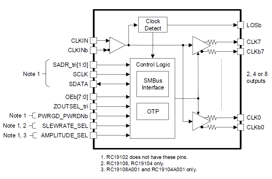
The RC19102 is a 1.8V 2-output PCIe Gen7 buffer that is backward compatible with earlier PCIe generations. The RC19102 provides ultra-low additive jitter and reduced in-to-out delay performance for better design margin and incorporates several features for easier and more robust design.