Overview
Description
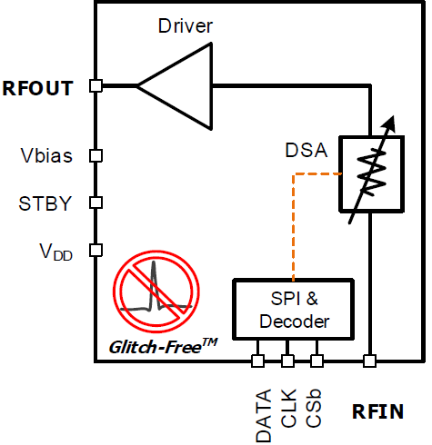
The F1431B is a high linearity RF Digital Variable Gain Amplifier, (DVGA) used as the power amplifier driver in transmitter applications. The F1431B provides 14dB gain, +41.1dBm OIP3, and a 4.2dB noise figure (NF) at 2.0GHz. The digital step attenuator (DSA) has a 23dB range with a 0.5dB step size and operates from 0.35GHz to 3GHz with one tuning circuit. This device uses a single 5V supply and 150mA of current.
Features
- 0.35GHz to 3GHz operating range
- 14.3dB typical gain at 2GHz
- Glitch-Free™ 23dB gain adjustment
- 0.5dB step size
- 4.2dB NF at 2GHz
- +41.1dBm OIP3 at 2GHz
- +23.3dBm output P1dB at 2GHz
- Single 5V supply voltage
- IDD = 150mA
- 50Ω single-ended input/output impedances
- 1.8V and 3.3V logic support
- Standby Mode for power savings
- Operating temperature (TCASE) range: -40 °C to +105 °C
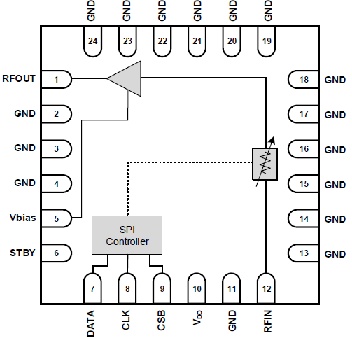
- 4mm × 4mm, 24-TQFN package
Comparison
Applications
Documentation
Featured Documentation
Log in required to subscribe
|
|
|
|
|---|---|---|
| Type | Title | Date |
| Datasheet | PDF 2.82 MB | |
1 item
|
||
Design & Development
Software & Tools
Boards & Kits
Evaluation
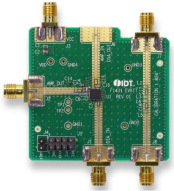
F1431BEVB
Active
Evaluation Board for the F1431B High Linearity RF DVGA
The F1431BEVB is a fully-populated evaluation board which allows the customer to easily evaluate the F1431B differential input amplifier. Component placement of the output matching components C5, L1, and C6 is critical and these components should be placed as close to pin 1 of the F1431B as...
Recommended Documents:
Models
ECAD Models
Schematic symbols, PCB footprints, and 3D CAD models from SamacSys can be found by clicking on the CAD Model links in the Product Options table. If a symbol or model isn't available, it can be requested directly from SamacSys.

Product Options
Applied Filters: