Package Information
| Pitch (mm) | 0.65 |
| Lead Count (#) | 16 |
| Pkg. Dimensions (mm) | 5.00 x 4.39 x 0.00 |
| Pkg. Code | MXX |
| Pkg. Type | TSSOP |
Environmental & Export Classifications
| Moisture Sensitivity Level (MSL) | 1 |
| Pb (Lead) Free | Yes |
| ECCN (US) | EAR99 |
| HTS (US) |
Product Attributes
| Lead Count (#) | 16 |
| Carrier Type | Reel |
| Moisture Sensitivity Level (MSL) | 1 |
| Pitch (mm) | 0.7 |
| Pkg. Dimensions (mm) | 5.0 x 4.4 x 0.00 |
| Pb (Lead) Free | Yes |
| Pb Free Category | Pb-Free 100% Matte Tin Plate w/Anneal-e3 |
| Temp. Range | -40 to +85°C |
| Channels (#) | 2 |
| Charge Injection (pC) | 60 |
| Configuration | NO |
| Drain Capacitance | 39 pF |
| IS (mA) | 1E-05 |
| Leakage (nA) | 0.04 |
| Length (mm) | 5 |
| MOQ | 2500 |
| Pkg. Type | TSSOP |
| Qualification Level | Standard |
| RDS (ON) (Ohms) | 20 |
| Source Cap (pf) | 12 |
| Supply Voltage Vcc Range | 5 to 34, ±5 to ±20 |
| Switch or MUX | Switch |
| TOFF (ns) | 60 |
| TON (ns) | 100 |
| Thickness (mm) | 0 |
| Type of Switch | SPST |
| VCC (Single) (V) | 5 - 34 |
| Width (mm) | 4.4 |
Description
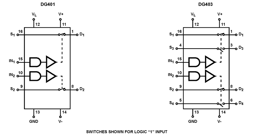
The DG401 and DG403 monolithic CMOS analog switches have TTL and CMOS compatible digital inputs. These switches feature low analog ON resistance (45Ω) and fast switch time (tON150ns). Low charge injection simplifies sample and hold applications. The improvements in the DG401, DG403 series are made possible by using a high voltage silicon-gate process. An epitaxial layer prevents the latch-up associated with older CMOS technologies. The 44V maximum voltage range permits controlling 30VP-P signals. Power supplies may be single-ended from +5V to +34V, or split from ±5V to ±17V. The analog switches are bilateral, equally matched for AC or bidirectional signals. The ON resistance variation with analog signals is quite low over a ±15V analog input range. The three different devices provide the equivalent of two SPST (DG401) or two SPDT (DG403) relay switch contacts with CMOS or TTL level activation. The pinout is similar, permitting a standard layout to be used, choosing the switch function as needed.
