Overview
Description
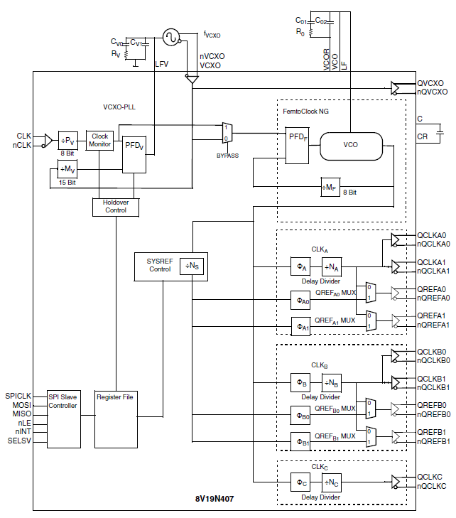
The 8V19N407Z-24 is a fully integrated FemtoClock® NG jitter attenuator and clock synthesizer. The device is a high-performance clock solution for conditioning and frequency/phase management of wireless base station radio equipment boards and is optimized to deliver excellent phase noise performance. This device supports JESD204B subclass 0 and 1 clock implementations. It is very flexible in the programming of the output frequency and phase. A two-stage PLL architecture supports both jitter attenuation and frequency multiplication. The first stage PLL is the jitter attenuator and uses an external VCXO for best possible phase noise characteristics. The first stage PLL lock on the VCXO-PLL output signal and synthesizes the target frequency. The second stage PLL uses an internal VCO.
The device supports the clock generation of high-frequency clocks from the VCO and low-frequency system reference signals (SYSREF). The system reference signals are internally synchronized to the clock signals. Delay functions exist for achieving alignment and controlled phase delay between system reference and clock signals and to align/delay individual output signals. The input is monitored for activity. The "hold-over" is provided to handle clock input failure scenarios. Auto-lock, individually programmable output frequency dividers, and phase adjustment capabilities are added for flexibility. The device is configured through a 4-wire SP serial interface and reports lock and signal loss status in internal registers and optionally via a lock detect (nINT) output. The device is packaged in a lead-free (RoHS 6) 72-lead VFQFN package. The extended temperature range supports wireless infrastructure, telecommunication, and networking end equipment requirements.
Features
- Core timing unit for JESD204B wireless infrastructure and Ethernet clocks
- First stage PLL uses an external VCXO for jitter attenuation
- Second PLL stage facilitates an integrated VCO for frequency synthesis
- 8V19N407-19: fVCO = 1900 - 2000MHz
- 8V19N407-24: fVCO = 2400 - 2500MHz
- Five differential configurable LVPECL, LVDS clock outputs with a variable output amplitude
- Four differential LVDS system reference (SYSREF) signal outputs
- Synchronization between clock and system reference signals
- Wide input frequency range supported by 8-bit pre- and 15-bit VCXO-PLL feedback divider
- Output clock frequencies: fVCO ÷ N
- Three independent output clock frequency dividers N (range of ÷1 to ÷96)
- Phase delay capabilities for alignment/delay for clock and SYSREF signals
- Individual output phase adjustment (Clock): One period of the selected VCO frequency in 64 steps
- Individual output phase adjustment (SYSREF): Approximately a half period of the selected VCO frequency in 8 steps
- Internal, SPI-controlled SYSREF pulse generation
- SYSREF frequencies: fVCO ÷ NS
- SYSREF frequency dividers NS: ÷64 to ÷2048 (10 dividers)
- Clock input compatible with LVPECL, LVDS, and LVCMOS signals
- Dedicated power-down features for reducing power consumption
- Input clock monitoring
- Holdover for temporary loss of input signal scenarios
- Support of output power-down and output disable
- Typical clock output phase noise at 307.2MHz: 1MHz offset: -154.6 dBc/Hz
- Typical clock output phase noise at 156.25 MHz: 1MHz offset: -158.4 dBc/Hz
- RMS phase noise of 307.2 MHz clock (12kHz - 20MHz): 81.3fs (typical)
- RMS phase noise of 156.25 MHz clock (12kHz - 20MHz): 83.7fs (typical)
- Status conditions with programmable functionality for loss-of-lock and loss-of-reference indication
- Lock detect (nINT) output for status change indication
- 3.3V core and output supply mode
- -40 °C to +85 °C ambient operating temperature
- Lead-free (RoHS 6) 72-lead VFQFN package
Comparison
Applications
Design & Development
Models
ECAD Models
Schematic symbols, PCB footprints, and 3D CAD models from SamacSys can be found by clicking on the CAD Model links in the Product Options table. If a symbol or model isn't available, it can be requested directly from SamacSys.

Product Options
Applied Filters:
Videos & Training
News & Blog Posts
Blog Post
Apr 27, 2021
|