Package Information
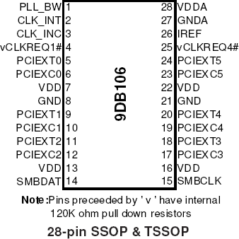
| Lead Count (#) | 28 |
| Pkg. Dimensions (mm) | 10.2 x 5.3 x 1.73 |
| Pkg. Code | PYG28 |
| Pitch (mm) | 0.65 |
| Pkg. Type | SSOP |
Environmental & Export Classifications
| Moisture Sensitivity Level (MSL) | 1 |
| Pb (Lead) Free | Yes |
| ECCN (US) | NLR |
| HTS (US) | 8542390001 |
Product Attributes
| Lead Count (#) | 28 |
| Carrier Type | Reel |
| Moisture Sensitivity Level (MSL) | 1 |
| Qty. per Reel (#) | 1500 |
| Qty. per Carrier (#) | 0 |
| Package Area (mm²) | 54.1 |
| Pkg. Dimensions (mm) | 10.2 x 5.3 x 1.73 |
| Pb (Lead) Free | Yes |
| Pb Free Category | e3 Sn |
| Temp. Range | 0 to 70°C |
| Accepts Spread Spec Input | Yes |
| App Jitter Compliance | PCIe Gen1, PCIe Gen2 |
| Architecture | Common |
| C-C Jitter Max P-P (ps) | 50 |
| C-C Jitter Typ P-P (ps) | 35 |
| Core Voltage (V) | 3.3 |
| Diff. Input Signaling | HCSL |
| Diff. Inputs | 1 |
| Diff. Output Signaling | HCSL |
| Diff. Outputs | 6 |
| Diff. Termination Resistors | 24 |
| Feedback Input | No |
| Function | Zero Delay Buffer |
| Input Freq (MHz) | 100 - 100 |
| Input Type | HCSL |
| Inputs (#) | 1 |
| Length (mm) | 10.2 |
| MOQ | 1500 |
| Output Banks (#) | 1 |
| Output Freq Range (MHz) | 80 - 105 |
| Output Skew (ps) | 50 |
| Output Type | HCSL |
| Output Voltage (V) | 3.3 |
| Outputs (#) | 6 |
| PLL | Yes |
| Phase Jitter Max RMS (ps) | 3.000 |
| Phase Jitter Typ RMS (ps) | 1.300 |
| Pitch (mm) | 0.65 |
| Pkg. Type | SSOP |
| Power Consumption Typ (mW) | 429 |
| Prog. Clock | No |
| Prog. Interface | SMBUS |
| Reel Size (in) | 13 |
| Requires Terms and Conditions | Does not require acceptance of Terms and Conditions |
| Supply Voltage (V) | 3.3 - 3.3 |
| Tape & Reel | Yes |
| Thickness (mm) | 1.73 |
| Width (mm) | 5.3 |
Resources for 9DB106
Description
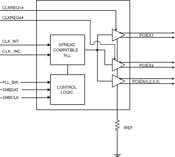
The 9DB106 zero-delay buffer supports PCIe Gen1 and Gen2 clocking requirements. The 9DB106 is driven by a differential SRC output pair from an IDT CK410/CK505-compliant main clock generator. It attenuates jitter on the input clock and has a selectable PLL bandwidth to maximize performance in systems with or without Spread-Spectrum clocking. An SMBus interface allows control of the PLL bandwidth and bypass options, while 2 clock request (CLKREQ#) pins make the 9DB106 suitable for Express Card applications.

