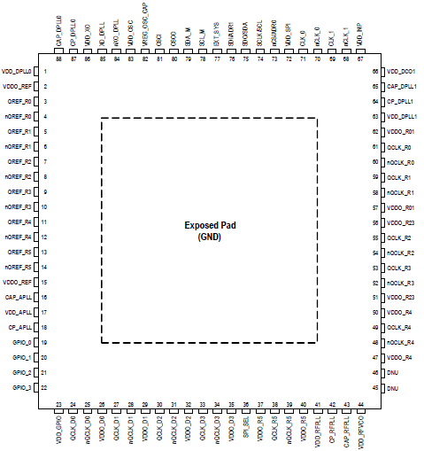
| Lead Count (#) | 88 |
| Pkg. Code | NLG88 |
| Pitch (mm) | 0.4 |
| Pkg. Type | VFQFPN |
| Pkg. Dimensions (mm) | 10.0 x 10.0 x 0.9 |
| Moisture Sensitivity Level (MSL) | 3 |
| Pb (Lead) Free | Yes |
| ECCN (US) | NLR |
| HTS (US) | 8542390001 |
| Lead Count (#) | 88 |
| Carrier Type | Reel |
| Moisture Sensitivity Level (MSL) | 3 |
| Qty. per Reel (#) | 2500 |
| Qty. per Carrier (#) | 0 |
| Pb (Lead) Free | Yes |
| Pb Free Category | e3 Sn |
| Temp. Range | -40 to +85°C |
| Country of Assembly | Taiwan |
| Country of Wafer Fabrication | United States |
| Accepts Spread Spec Input | No |
| Additive Phase Jitter Typ RMS (fs) | 52 |
| Additive Phase Jitter Typ RMS (ps) | 0.052 |
| Adjustable Phase | Yes |
| Advanced Features | eEEC, T-BC, T-TSC Class C, 1PPS, DCO, IEEE 1588, JESD204B, JESD204C |
| Channels (#) | 1 |
| Core Voltage (V) | 1.8 |
| DPLL Channels (#) | 2 |
| Feedback Divider Resolution (bits) | 32 |
| Fractional Output Dividers (#) | 0 |
| Frequency Plan | 2500 / Output_Divider, 2949.12 / Output_Divider, 3670-3868 / Output_Divider |
| Grade | 5G |
| Input Freq (MHz) | 0.000001 - 1000 |
| Input Redundancy | Input Monitor, Digital holdover, Hitless switch, Phase-slope limiting |
| Input Ref. Divider Resolution (bits) | 3 |
| Inputs (#) | 2 |
| JESD204B/C Compliant | Yes |
| Length (mm) | 10 |
| Loop Bandwidth Range (Hz) | 20 - 100 |
| MOQ | 2500 |
| Noise Floor (dBc/Hz) | -165 |
| Output Banks (#) | 8 |
| Output Divider Resolution (bits) | 7 |
| Output Freq Range (MHz) | 0.000001 - 1000 |
| Output Skew (ps) | 74 |
| Output Type | LVDS, LVPECL, LVCMOS |
| Output Voltage (V) | 1.8, 2.5, 3.3 |
| Outputs (#) | 16 |
| PLL | Yes |
| Phase Jitter Typ RMS (fs) | 74.000 |
| Phase Jitter Typ RMS (ps) | 0.074 |
| Phase Noise Supports GSM | Yes |
| Pitch (mm) | 0.4 |
| Pkg. Dimensions (mm) | 10.0 x 10.0 x 0.9 |
| Pkg. Type | VFQFPN |
| Ports (#) | 1 |
| Prog. Clock | Yes |
| Reel Size (in) | 13 |
| Supply Voltage (V) | 3.3 - 3.3, 2.5 - 2.5, 1.8 - 1.8 |
| Synthesis Mode | Integer, Fractional |
| Tape & Reel | Yes |
| Thickness (mm) | 0.9 |
| Width (mm) | 10 |
| Xtal Freq (KHz) | 15000 - 500000 |
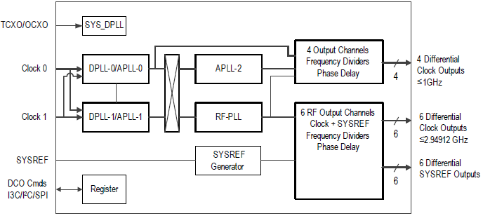
The 8V19N850 is a fully integrated Radio Unit Clock Synchronizer and Jitter Attenuator designed as a high-performance clock solution for phase/frequency synchronization and signal conditioning of wireless base station radio equipment. The device supports JESD204B/C subclass 0 and 1 device clocks and SYSREF synchronization for converters. The 8V19N850 supports two independent frequency domains: one that can be used for the digital clock (Ethernet and FEC rates) domain with four outputs, and the device clock (RF-PLL) domain with 12 outputs. The Ethernet domain generates frequencies from two independent APLLs for flexibility; the outputs of the RF clock domain generate very low phase noise clocks for ADC/DAC circuits.
From the integrated RF-PLL, the device supports the clock generation of high-frequency device clocks for driving ADC/DAC devices low-frequency synchronization signals (SYSREF). A dual DPLL front-end architecture supports any frequency translation. Each DPLL provides a programmable bandwidth and a DCO function for real-time frequency/phase adjustments. The DPLLs can lock on 1PPS input signals and establish lock within 100s or less. Frequency information can be applied from DPLL-0 to DPLL-1 and vice versa to enable the combining of the frequency characteristics of two references (combo-mode). The 8V19N850 is configured through a pin-mapped I3C (including legacy I2C) and 3/4-wire SPI interface. I2C with master capabilities reads a default configuration from an external ROM device. GPIO ports can be configured for reporting and controlling purposes.