Features
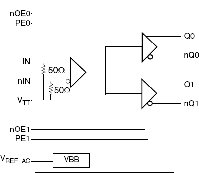
- 1:2 differential data/clock fanout buffer and line driver
- 4.5 Gbps data rate (NRZ) (maximum)
- Differential LVDS outputs
- Differential input supporting LVDS, LVPECL and CML levels
- Configurable output pre-emphasis
- Low-skew outputs: 10ps (maximum)
- Low data deterministic jitter: 4ps (maximum)
- LVCMOS interface levels for the control inputs
- Asynchronous output disable into high-impedance state
- Internal input termination: 100? (Differential)
- Additive phase jitter, RMS: 0.08ps (typical)
- Full 3.3V supply voltage
- -40°C to 85°C ambient operating temperature
- Available in lead-free (RoHS 6) package
Description
The 854S712I is a differential, high-speed 1:2 data/clock fanout buffer and line driver. The outputs support pre-emphasis in order to drive backplanes and long transmission lines while reducing inter-symbol interference effects. The pre-emphasis level is configurable to optimize for low bit error rate or power consumption. Pre-emphasis utilizes an increased output voltage swing for transition bits. The device is optimized for data rates up to 4.5 Gbps (NRZ) and for deterministic jitter in data applications and low additive jitter in clock applications. The outputs are LVDS-compliant while the differential input is compatible with a variety of signal levels such as LVDS, LVPECL and CML. Internal input termination, a bias voltage output for AC-coupling and small packaging (VFQFN) supports space-efficient board designs. The 854S712I operates from a 3.3V power supply and supports the industrial temperature range of -40°C to +85°C.
Parameters
| Attributes | Value |
|---|---|
| Function | Buffer |
| Outputs (#) | 2 |
| Output Type | LVDS |
| Output Freq Range (MHz) | 3000 |
| Input Type | CML, LVDS, LVPECL |
| Output Banks (#) | 1 |
| Output Voltage (V) | 3.3 |
| Output Skew (ps) | 10 |
| Additive Phase Jitter Typ RMS (fs) | 80 |
| Advanced Features | Output pre-emphasis |
Package Options
| Pkg. Type | Pkg. Dimensions (mm) | Lead Count (#) | Pitch (mm) |
|---|---|---|---|
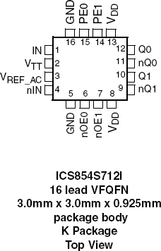
| VFQFPN | 3.0 x 3.0 x 1.0 | 16 | 0.5 |
Applied Filters:


