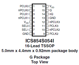
| Lead Count (#) | 16 |
| Pkg. Code | PGG16 |
| Pitch (mm) | 0.65 |
| Pkg. Type | TSSOP |
| Pkg. Dimensions (mm) | 5.0 x 4.4 x 1.0 |
| Moisture Sensitivity Level (MSL) | 1 |
| Pb (Lead) Free | Yes |
| ECCN (US) | NLR |
| HTS (US) | 8542390001 |
| Lead Count (#) | 16 |
| Carrier Type | Tube |
| Moisture Sensitivity Level (MSL) | 1 |
| Qty. per Reel (#) | 0 |
| Qty. per Carrier (#) | 96 |
| Pb (Lead) Free | Yes |
| Pb Free Category | e3 Sn |
| Temp. Range | -40 to +85°C |
| Additive Phase Jitter Typ RMS (fs) | 147 |
| Additive Phase Jitter Typ RMS (ps) | 0.147 |
| Core Voltage (V) | 3.135 |
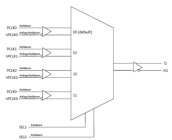
| Function | Multiplexer |
| Input Freq (MHz) | 0 - 2500 |
| Input Type | LVPECL, LVDS, CML |
| Inputs (#) | 4 |
| Length (mm) | 5 |
| MOQ | 96 |
| Output Banks (#) | 1 |
| Output Freq Range (MHz) | 0 - 2500 |
| Output Signaling | LVDS |
| Output Type | LVDS |
| Output Voltage (V) | 3.3 |
| Outputs (#) | 1 |
| Package Area (mm²) | 22.0 |
| Pitch (mm) | 0.65 |
| Pkg. Dimensions (mm) | 5.0 x 4.4 x 1.0 |
| Pkg. Type | TSSOP |
| Requires Terms and Conditions | Does not require acceptance of Terms and Conditions |
| Tape & Reel | No |
| Thickness (mm) | 1 |
| Width (mm) | 4.4 |
The 854S054I is a 4:1 differential-to-LVDS clock multiplexer that can operate up to 2.5GHz. The 854S054I has four selectable differential clock inputs. The PCLK, nPCLK input pairs can accept LVPECL, LVDS, or CML levels. The fully differential architecture and low propagation delay make it ideal for use in clock distribution circuits. The select pins have internal pull-down resistors. The SEL1 pin is the most significant bit and the binary number applied to the select pins will select the same numbered data input (i.e., 00 selects PCLK0, nPCLK0).