Overview
Description
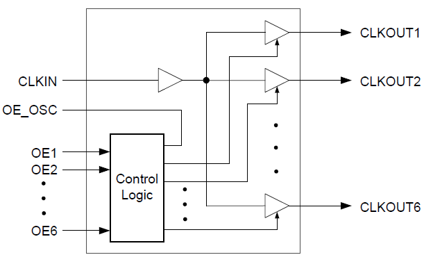
The 5PB1206 is a high-performance TCXO/LVCMOS clock fanout buffer with individual OE pins for each output. The CLKIN pin can accept either a square wave (LVCMOS) or a clipped sine wave (such as TCXO clipped sine wave output) as input.
The 5PB1206 has industry-leading low jitter and extremely low current consumption, making it ideal for smart mobile devices.
Features
- Extremely low operating and standby current consumption
- Low RMS Additive Phase jitter
- 1.8V power supply voltage
- Six outputs with individual Output Enable pin
- One input
- OE_OSC control pin to enable/disable reference TCXO/XO
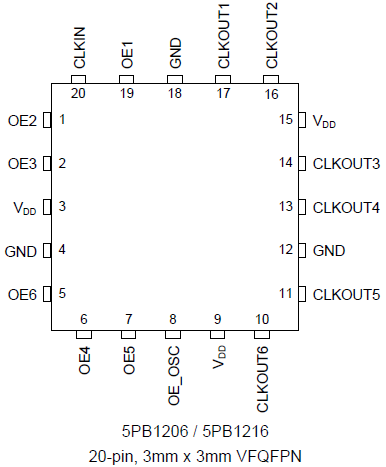
- Small 20-pin VFQFPN package
- Extended temperature range (-40 °C to +105 °C)
Comparison
Applications
Design & Development

Support

Support Communities
Get quick technical support online from Renesas Engineering Community technical staff.


Videos & Training
This video provides an overview of the LVCMOS High Performance Clock Buffer Family, highlighting their key features and capabilities.
Related Resources
News & Blog Posts
News
Mar 24, 2015
|