Overview
Description
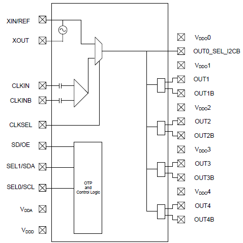
The 5P1105 is a programmable fanout buffer intended for high-performance consumer, networking, industrial, computing, and data communications applications. Configurations may be stored in on-chip One-Time Programmable (OTP) memory or changed using the I²C interface.
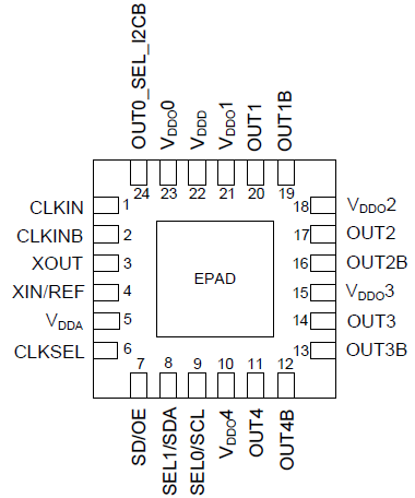
The outputs are generated from a single reference clock. The reference clock can come from one of the two redundant clock inputs. A glitchless manual switchover function allows one of the redundant clocks to be selected during normal operation. Two select pins allow up to four different configurations to be programmed and accessible using processor GPIOs or bootstrapping. The device is available in a 24-pin VFQFPN 4mm x 4mm package, with an industrial operating temperature range of -40 °C to +85 °C.
Features
- Up to four high-performance universal differential output pairs:
- Low RMS additive phase jitter: 0.2ps
- Four banks of internal non-volatile in-system programmable or factory programmable OTP memory
- I²C serial programming interface
- One additional LVCMOS output clock
- Four universal output pairs:
- Each configurable as one differential output pair or two LVCMOS outputs
- I/O standards:
- Single-ended I/Os: 1.8V to 3.3V LVCMOS
- Differential I/Os: LVPECL, LVDS, and HCSL
- Input frequency ranges:
- LVCMOS reference clock input (XIN/REF) – 1MHz to 200MHz
- LVDS, LVPECL, HCSL differential clock input (CLKIN, CLKINB) – 1MHz to 350MHz
- Crystal frequency range – 8MHz to 40MHz
- Individually selectable output voltage (1.8V, 2.5V, 3.3V) for each output pair
- Redundant clock inputs with manual switchover
- Programmable crystal load capacitance
- Individual output enable/disable
- Power-down mode
- 1.8V, 2.5V, or 3.3V core VDDD, VDDA
Comparison
Applications
Design & Development
Software & Tools
Boards & Kits
Models
ECAD Models
Schematic symbols, PCB footprints, and 3D CAD models from SamacSys can be found by clicking on the CAD Model links in the Product Options table. If a symbol or model isn't available, it can be requested directly from SamacSys.

Support

Support Communities
Get quick technical support online from Renesas Engineering Community technical staff.


Resources
Support Communities
-
5P1105 - should RAM register changes take affect immediately?
... bit address). I connected a Raspberry Pi to it via I2C and the AARDVARK connector, and it can see and manipulate the registers of the 5P1105, so the inability of Timing Commander to connect is an inconvenience rather than a fatal problem. On to my immediate question: should changes to ...
Oct 1, 2024 -
Is there an schematic for EVK-5P1105 rev B?
All the online documentation I have found is for Rev A of the board, and Rev B has some extra jumpers.
Sep 25, 2024 -
I want to find a replacement for 844021BG-01LF, input 25MHz clock, output 125MHz LVDS clock
I want to find a replacement for 844021BG-01LF, input 25MHz clock, output 125MHz LVDS clock
Mar 9, 2022
FAQs
-
5P1105 Programming Part Number Options
The 5P1105 family is a programmable fanout buffer. 5P1105A000NLGI8 is the generic, unprogrammed part. Customers can request special configurations from the factory and a special version of the part will be created (a number will be assigned in place of 000). These parts programmed at the factory for customers, you ...
Oct 18, 2021