Introduction to Electronic Circuits: 3 of 3
In this session we look at operational amplifiers ("op-amps") and their uses in amplifiers and comparators.
Op-Amps: Ubiquitous ICs with Multiple Applications
An op-amp operates on analog input. It can be used to amplify or attenuate this input, and to carry out mathematical operations such as addition, subtraction, integration, and differentiation. Because of their wide range of uses, op-amps are encountered in most electric circuits.
A typical op-amp, such as shown in Figure 1, is equipped with a non-inverting input (Vin (+)), an inverting input (Vin (−)), and an output (Vout). Although not shown in the diagram, an op-amp also has two power inputs (positive and negative), and may also include an offset input and other terminals.
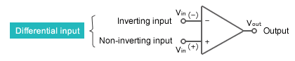
Figure 1: Op-amp Circuit
The fundamental function of an op-amp is to greatly amplify the differential between the two inputs, and output the result. If input at V(+) is greater than at V(−), the op-amp will amplify and output a positive signal; if V(−) is greater, the op-amp will output an amplified negative signal. Two other features of a typical op-amp are: (a) the input impedance is extremely high, and (b) the output impedance is extremely low.
Because the op-amp's gain is so high, even small differences in the inputs will rapidly drive the output voltage to its maximum or minimum value. For this reason, op-amps are usually connected to a negative feedback. Let's look at an example.
Op-Amp Basics (1): An Inverting Amplifier Circuit
The circuit shown in Fig. 2 amplifies and inverts (reverses the phase of) the input signal, and outputs the result. The circuit uses negative feedback: some of the output signal is inverted and returned to the input. In this example, feedback occurs because output Vout is connected through resistor R2 to the inverting input (−).
Let's look at how this circuit works. If the output is not connected to a power voltage, then the voltages applied to the inverting (−) and non-inverting (+) inputs are equal; the two inputs act as if shorted together; we can envision an imaginary short. Since the voltage difference between this imaginary short and the non-inverting input is 0 V, point A will also be at 0 V. By Ohm's Law, then, we have I1 = Vin/R1.
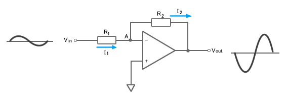
Figure 2: Inverting Amplifier Circuit
Because op-amps have extremely high input impedance, there is virtually no current flow into the inverting input (−). Accordingly, I1 flows through point A and R2; this means that I1 and I2 are virtually equal. Then, by Ohm's Law, we have Vout = −I1 × R2, where I1 is negative because I2 flows from point A, where the voltage is 0. Looking at this in another way: any attempt to raise the input voltage at the inverting input (−) produces inverted and highly amplified output voltage that flows backward, passing through R2 and connecting to the inverted input terminal (−), thereby suppressing the voltage rise at this terminal. The system stabilizes at the output voltage that brings the voltage at the inverting input (−) to 0 V, equivalent to the voltage at the non-inverting input.
Next, let's see how we can use the relationship between input and output to find the op-amp's gain. Specifically, Vout/Vin = (−I1 × R2) / (I1 × R1) = −R2/R1. The gain is negative because the output waveform phase is opposite that of the input waveform.
An important thing to note about the above equation is that the gain is entirely determined by the ratio of resistances R2 and R1. Accordingly, you can change the gain simply by changing the resistances. So while the op-amp itself has a high gain, appropriate use of negative feedback can reduce the actual amplification to the desired level.
Op-Amp Basics (2): Non-Inverting Amplifier Circuit
In the previous section we saw how an op-amp can be used to implement an inverting amplifier. Figure 3 shows how we can use it to make a non-inverting amplifier. The non-inverting amp differs from the inverting one in two major ways: (1) the output waveform is in phase with the input waveform, and (2) the input goes into the non-inverting input terminal (+). But note that non-inverting and inverting circuits both make use of negative feedback.
So how does this circuit work? We still have the imaginary short, which means that the non-inverting (+) and inverting (−) inputs are both at voltage Vin. So point A is also at Vin. Ohm's Law tells us that the voltage at R1 is Vin = R1 × I1. And since there is essentially no current into either of the op-amp inputs, it follows that I1 = I2. And as Vout is the sum of voltages at R1 and R2, we know that Vout= R2 × I2 + R1 × I1. We can rearrange these expressions to find the gain G, like this: G = Vout/Vin = (1 + R2/R1)
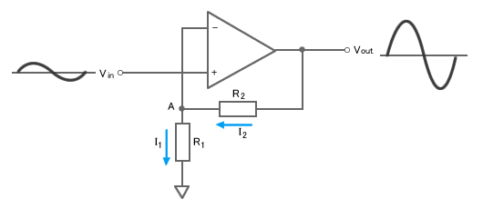
Figure 3: Non-inverting Amplifier Circuit
Because this amplifier preserves the phase, it is often found in applications where phase considerations are an issue.
Note also that if R1 is removed from the circuit and R2 is set to 0 ohm (or shorted), the circuit becomes a voltage follower with a gain of 1. This type of circuit is often used in buffering circuitry and impedance conversion circuits.
Comparator Circuit
A comparator circuit compares two voltages and outputs either a 1 (the voltage at the plus side; VDD in the illustration) or a 0 (the voltage at the negative side) to indicate which is larger. Comparators are often used, for example, to check whether an input has reached some predetermined value. In most cases a comparator is implemented using a dedicated comparator IC, but op-amps may be used as an alternative. Comparator diagrams and op-amp diagrams use the same symbols.
Figure 4 shows a comparator circuit. Note first that the circuit does not use feedback. The circuit amplifies the voltage difference between Vin and VREF, and outputs the result at Vout. If Vin is greater than VREF, then voltage at Vout will rise to its positive saturation level; that is, to the voltage at the positive side. If Vin is lower than VREF, then Vout, will fall to its negative saturation level, equal to the voltage at the negative side.
In practice, this circuit can be improved by incorporating a hysteresis voltage range to reduce its sensitivity to noise. The circuit shown in Fig. 5, for example, will provide stable operation even when the Vin signal is somewhat noisy.
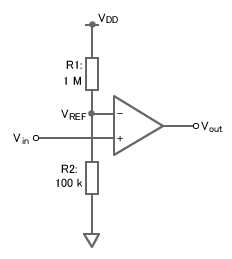
Figure 4: Comparator Circuit
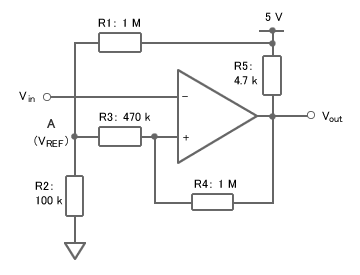
Figure 5: Comparator Circuit with Hysteresis
Oscillator Circuit Using Positive Feedback
Feedback refers to the return of a portion of a circuit's output back to the circuit input, for the purpose of regulating the circuit in some way. With negative feedback, higher feedback drives the circuit output down. With positive feedback, as in the example here, higher output drives the output up. When positive feedback is incorporated in a circuit with a positive gain, the circuit becomes an oscillator.
There are numerous types of oscillator circuits. Figure 6 shows an example of an astable multivibrator oscillator.
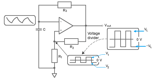
Figure 6: Astable Multivibrator Circuit
This circuit is called astable because it is unstable at both maximum voltages, voltage VL on the positive side, and −VL on the negative side, and will oscillate between these two levels. Let's look at how this circuit works. First, note that output Vout, goes through R2 and back into the op-amp's non-inverting terminal (+), forming a positive feedback circuit. Note also that Vout, R3, and C comprise an RC integrator circuit; or, to put it another way, that some of the voltage at Vout will gradually charges the capacitor.
At the beginning, the feedback circuit quickly drives Vout to its maximum positive output (equal to VL). But the R3 integrator circuit (R3 and C) gradually drives up the voltage on the inverting input terminal (−), until after a certain time this voltage becomes higher than the voltage at the non-inverting input terminal (+). When this occurs, a negative voltage gets input into the differential input, rapidly pushing Vout down to its negative-side maximum (−VL).
With Vout now on the negative side, however, the R3 integrator circuit begins to gradually drive up a negative voltage on the inverting terminal (−). And again, after a certain time, this negative voltage becomes greater than the voltage at the non-inverting terminal (+), causing the input of a positive voltage into the differential input, which rapidly pushes Vout back up to its positive side maximum (VL). This sequence continues to repeat, causing Vout to oscillate up and down between VL and − VL.
This has been the third and final session of our review of basic electronic circuits. We hope this review was helpful, even as we acknowledge that the scope was quite limited. Next time we begin our study of digital circuits. We look forward to your continued participation.
Module List
- Passive Elements
- Diodes, Transistors, and FETs
- Op-Amps, Comparator Circuit