Using the GreenPAK™ family of devices, it is easy to implement custom power sequencer designs in an extremely small area, using minimal power and board space. It is no secret that successfully powering up a system can be tricky as well as powering one off. Timing, order of events, and power levels need to be just right for proper system functionality and stability. Using a power sequencer can prevent unnecessary current draw while portions of the design sit idle, waiting for prerequisite systems to be powered. Some FPGAs, for example, may require more than ten rails, which if sequenced using discrete components, could introduce extra power and board space overhead. When paired with the tiny, ultra-low RDSON GreenFET™ load switch, power sequencing with our solution is incredibly efficient. Moreover, a power sequencer can be easily built on any GreenPAK IC.
Often in various combinations in a single system, some common methods for power sequencing include:
- Fixed timing
- Power Good
- I2C Acknowledge
- Voltage Sensing
GreenPAK Benefits for Power Sequencing
GreenPAK Enhances System Stability
- No code to avoid errors, hang-ups, or missed reset events
- Integration of many components ensuring fewer points of failure
GreenPAK Reduces Board Size
- Being as small as 1.2 mm² it is a perfect solution for mobile and wearable electronics.
GreenPAK Lowers Power Consumption
- GreenPAK can continuously run without ruining power budget
GreenPAK Maximizes GPIO Flexibility
- Configurable GPIO with Pull-up/down resistors, Push-Pull, Open drain, etc.
- Flexible GPIO routing to ensure the least complexity in PCB routing
- Integration of many common components to generate custom timing and logic to fit the requirements of many power sequencer designs
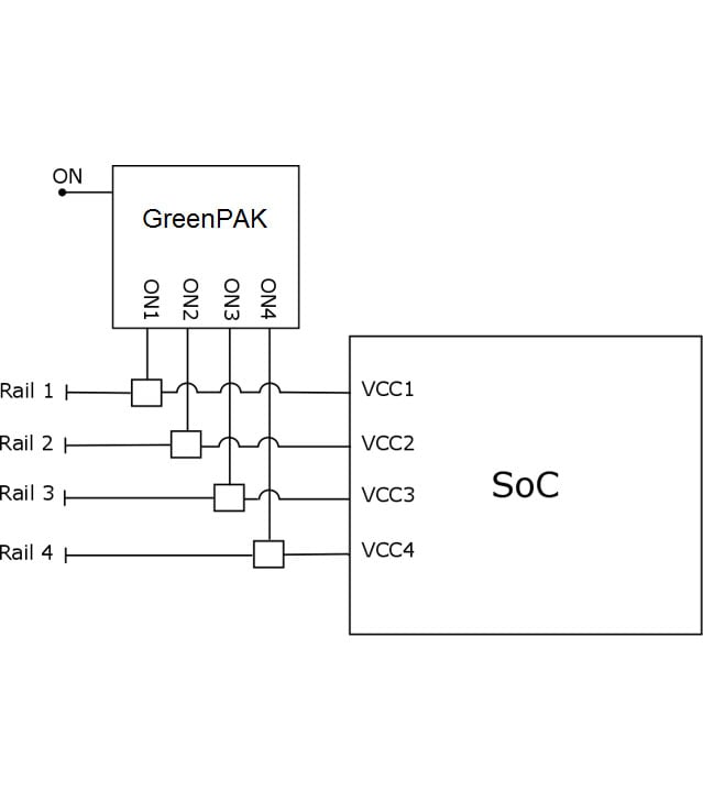
Fixed Delay Sequencing
One method for sequencing multiple sub-systems is to allot a fixed amount of time for each start-up sequence. This is appropriate for systems which do not feature a Power Good signal. Finding a discrete solution with the exact delay timings needed can take hours, but with GreenPAK's configurable logic and timing resources, developing a custom system is easy.
Example 1. Fixed Delay Sequencing
Key Design Considerations
Delay Time – Using GreenPAK's internal oscillators and CNT/DLY blocks, it is possible to address a wide range of timing requirements
ON Signal Polarity – GreenPAK can be configured to output active high or low using integrated inverters and LUTs
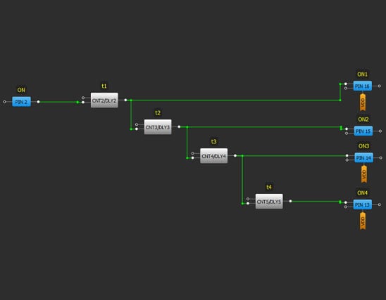
Example 1. GreenPAK Implementation
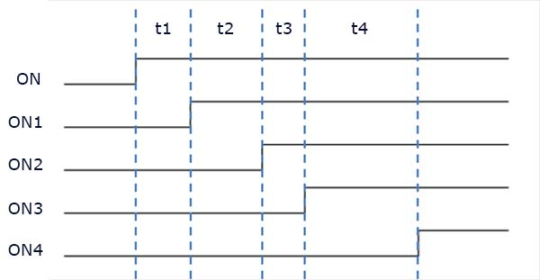
Example 1. Timing Diagram
Power Good
Many ICs have the ability to produce a Power Good (PG) signal once the respective systems have finished their start-up routine. This can be useful in systems where start-up time is not fixed and may depend on multiple variables.
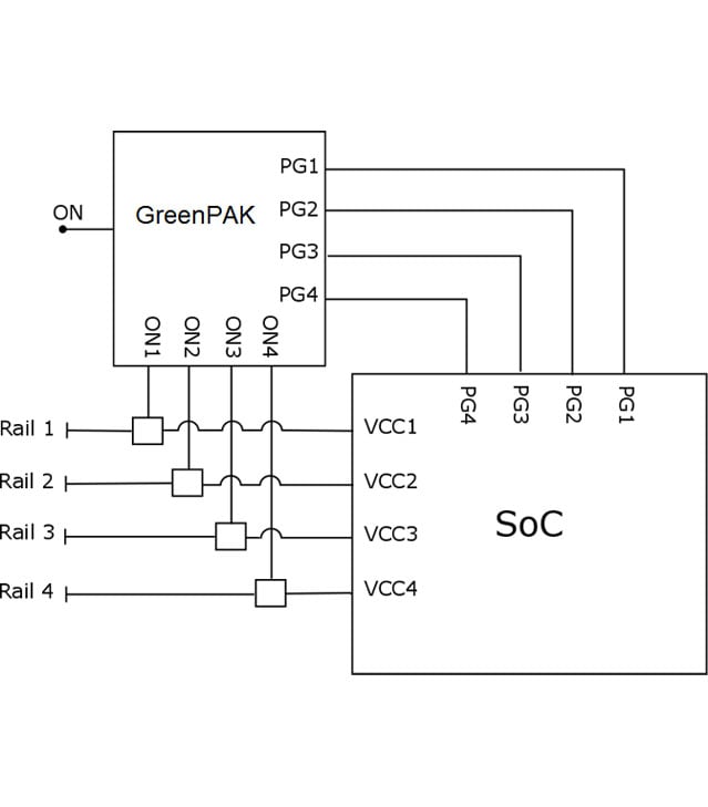
Example 2. Sequencing with Power Good
Key Design Considerations
ON and PG Signal Polarity - GreenPAK can be configured to output active high or low using integrated inverters and LUTs.
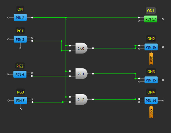
Example 2. GreenPAK Implementation
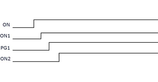
Example 2. Timing Diagram
I2C Acknowledge
Another option in programmable systems with I2C is to send a command to the power sequencer, in this case GreenPAK, to let it know start-up was completed successfully. Using GreenPAK's I2C virtual inputs, it is easy to treat an I2C command just like a digital Power Good signal.
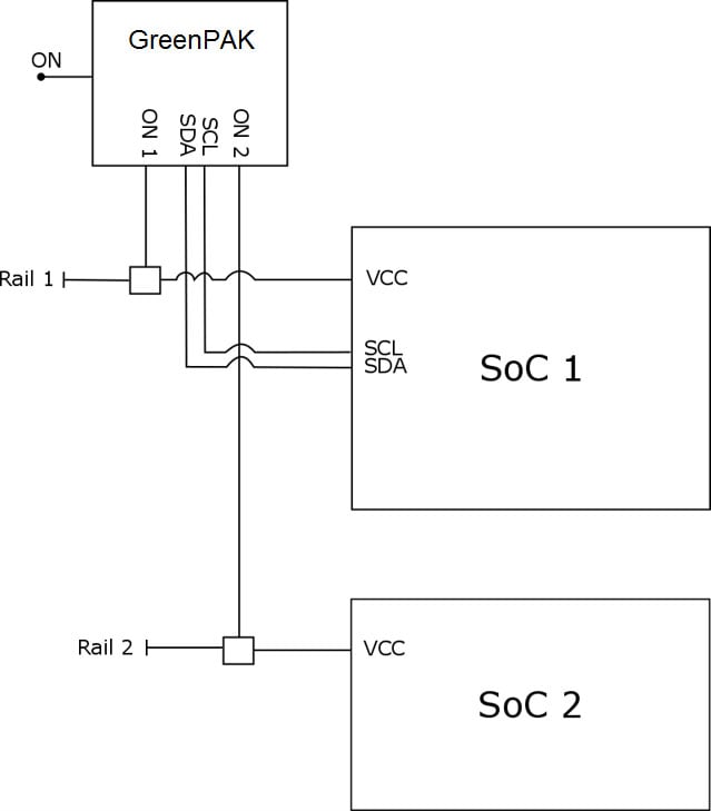
Example 3. Power Sequencer with I2C Acknowledge
Key Design Considerations
I2C Speed – GreenPAK I2C supports up to 400 kHz
I2C Address – GreenPAK can have up to 16 unique I2C addresses
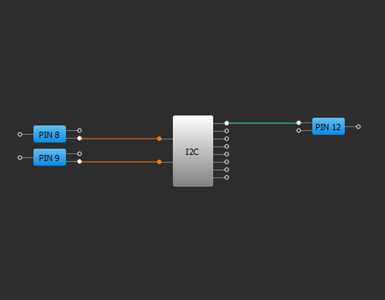
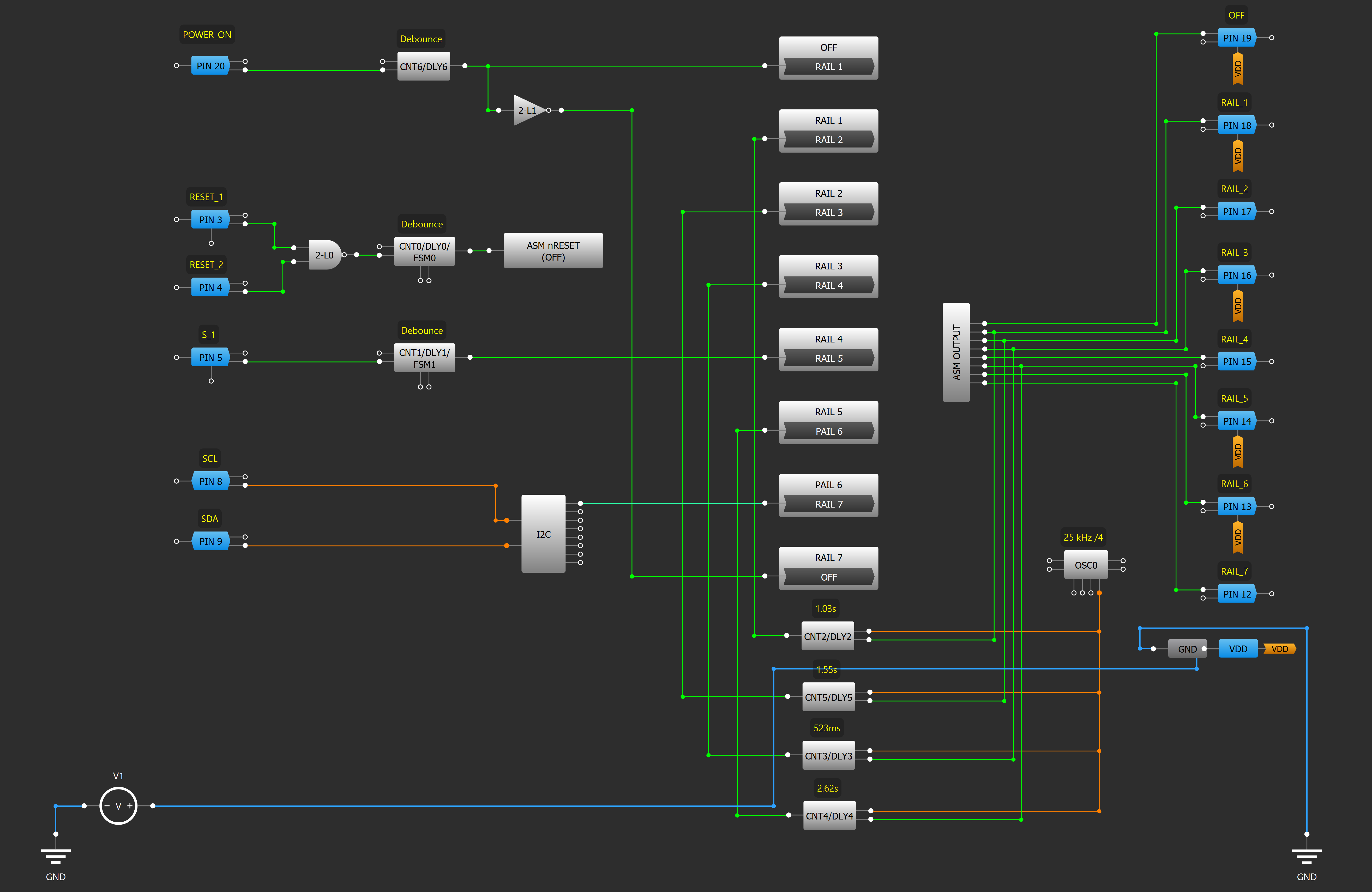
Example 3. GreenPAK Implementation
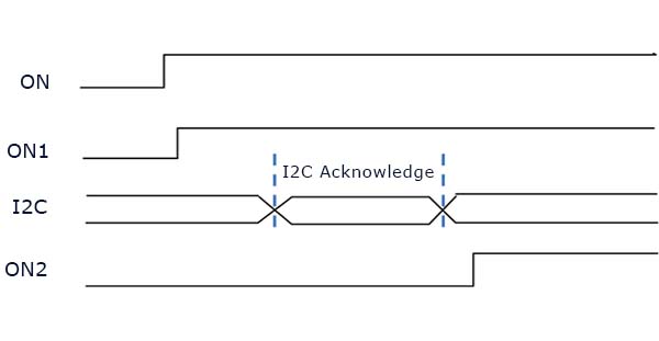
Example 3. Timing Diagram
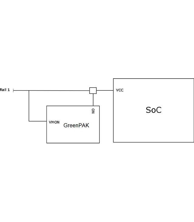
Voltage Sensing
To ensure system stability, many SOCs, DSPs, and FPGAs require a minimum voltage for startup. Monitoring the power level of a rail can be done simply using GreenPAK's configurable analog comparators.
Example 4. Power Sequencer with Voltage Sensing
Key Design Considerations
Over-voltage/Under-voltage Threshold – Supply tolerances vary, but using GreenPAK with integrated ACMPs enables reliable sequencing over a wide range of user-specified conditions
Time Sensitive Voltage Limits – Varying periods of voltages outside the limit may be tolerable for some systems. GreenPAK's configurable CNT/DLY blocks can be used to reject reset events below a wide range of time thresholds
Hysteresis – Nominal voltage requirements may incorporate hysteresis. GreenPAK's ACMPs can be configured with 25, 50, or 200 mV hysteresis
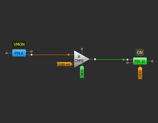
Example 4. GreenPAK Implementation
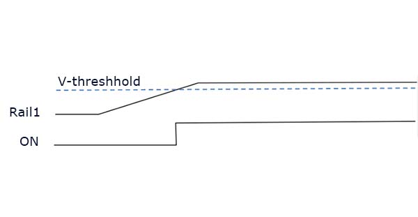
Example 4. Timing Diagram
GreenPAK Power Sequencer Demo Board is available for purchase. Please email us at [email protected] to learn more details.