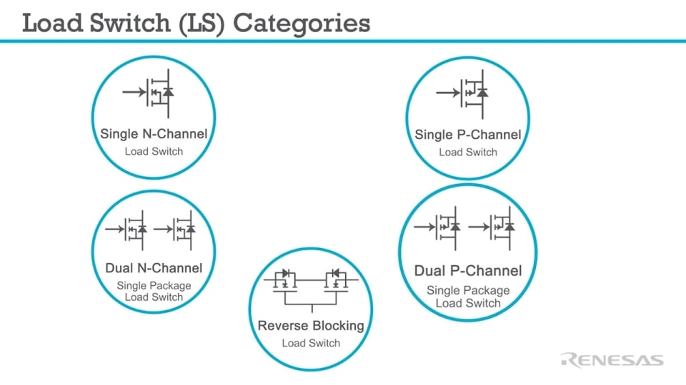
GreenFET high‑performance load switches are designed and optimized for high‑side power rail control applications from 0.25V to 25.2V where the load currents range from 1A to 9A.

Using a proprietary MOSFET design, all GreenFET load switches achieve ultra‑stable RDSON across wide input and supply voltage ranges. Combining proprietary MOSFET IP and advanced assembly techniques, these advanced state‑of‑the‑art products are available in ultra‑small PCB footprints from 0.56mm² to 5.04mm² and exhibit low thermal resistances for high‑current operation.

Compared to discrete FET circuit implementations, GreenFET products combine high‑performance nFET or pFET structures, high current handling capability, charge pumps, as well as multiple protection and control circuits into space‑efficient single- and dual‑channel products. The combination of all these advanced features directly results in BOM (bill‑of‑material) component and cost reductions as well as increasing system reliability and reduced board size.

All low- and high‑voltage GreenFET load switches are designed and fully characterized over the commercial (0 °C to 70 °C), extended commercial (-20 °C to 70 °C), industrial (-40 °C to 85 °C), or extended industrial (-40 °C to 125 °C) temperature ranges. Consistent with generating very low thermal gradients, Renesas load switches are available in low thermal resistance, STDFN/STQFN RoHS‑compliant packaging, and wafer‑level chip scale packaging (WLCSP).

Features

  • High‑performance nFET MOSFETs
    • Low RDSON: 13.3mΩ
    • Ultra-low ΔRDSON/ΔVIN: <0.05mΩ/V
    • Ultra-low ΔRDSON/ΔT: <0.06mΩ/°C
  • Internal protection features
    • Internal transient voltage suppressors (selected part numbers)
    • Automatic nFET SOA protection (5W and 10W options)
    • Pin-selectable overvoltage and undervoltage lockout windows
    • Fixed and capacitor-adjustable inrush current control
    • Fixed and resistor-adjustable current limit
    • Internal short-circuit current limit
    • Thermal shutdown
    • Fast VOUT discharge
  • Open-drain FAULT signaling
  • Open-drain Power Good signaling
  • MOSFET IDS analog current or power output load monitors (selected part numbers)
  • UL2367 certified (selected part numbers)

Applications

  • USB Type C high-end smartphones and tablet PCs
  • Point-of-Load power distribution in 5V, 12V, 15V, and 20V systems
  • Enterprise computing and telecom equipment
  • Multifunction printers
  • Fan motor drives
  • Enterprise copiers
  • Set-top boxes
  • General-purpose, high-voltage power rail switching
  • PCIe/PCI adapter cards

Documentation

Type Title Date
Application Note PDF 904 KB
Application Note PDF 736 KB
Guide PDF 3.47 MB
Overview PDF 5.26 MB
Application Note PDF 1.15 MB
Application Note PDF 888 KB
Training ZIP 50.42 MB 日本語 , 简体中文
Training ZIP 11.20 MB
Training ZIP 63.92 MB 日本語 , 简体中文
Training ZIP 12.44 MB
Application Note PDF 1.27 MB
Application Note PDF 911 KB
Application Note PDF 1.41 MB
Application Note PDF 364 KB
Application Note PDF 1.07 MB
Application Note PDF 609 KB
Application Note PDF 409 KB
Application Note PDF 278 KB
Application Note PDF 334 KB
Application Note PDF 482 KB
Application Note PDF 301 KB
Application Note ZIP 1.28 MB 日本語
Application Note PDF 847 KB
Application Note PDF 85 KB
Application Note PDF 980 KB
Application Note PDF 299 KB 简体中文
Application Note PDF 161 KB
27 items

Downloads

Type Title Date
PCB Design Files ZIP 65 KB
PCB Design Files ZIP 9 KB
PCB Design Files ZIP 221 KB
PCB Design Files ZIP 23 KB
PCB Design Files ZIP 2 KB
PCB Design Files ZIP 61 KB
6 items