Overview
Description
The AT25SF321 serial interface Flash memory device is designed for use in a wide variety of high-volume consumer based applications in which program code is shadowed from Flash memory into embedded or external RAM for execution. The flexible erase architecture of the AT25SF321 is ideal for data storage as well, eliminating the need for additional data storage devices.
The erase block sizes of the AT25SF321 have been optimized to meet the needs of today's code and data storage applications. By optimizing the size of the erase blocks, the memory space can be used much more efficiently. Because certain code modules and data storage segments must reside by themselves in their own erase regions, the wasted and unused memory space that occurs with large block erase Flash memory devices can be greatly reduced. This increased memory space efficiency allows additional code routines and data storage segments to be added while still maintaining the same overall device density.
The device also contains three pages of Security Register that can be used for purposes such as unique device serialization, system-level Electronic Serial Number (ESN) storage, locked key storage, etc. These Security Register pages can be individually locked.
Features
- Single 2.5V - 3.6V Supply
- Serial Peripheral Interface (SPI) Compatible
- Supports SPI Modes 0 and 3
- Supports Dual and Quad Output Read
- 104MHz Maximum Operating Frequency
- Clock-to-Output (tV) of 6ns
- Flexible, Optimized Erase Architecture for Code + Data Storage Applications
- Uniform 4-Kbyte Block Erase
- Uniform 32-Kbyte Block Erase
- Uniform 64-Kbyte Block Erase
- Full Chip Erase
- Hardware Controlled Locking of Protected Blocks via WP Pin
- 3 Protected Programmable Security Register Pages
- Flexible Programming
- Byte/Page Program (1 to 256 Bytes)
- Fast Program and Erase Times
- 0.7ms Typical Page Program (256 Bytes) Time
- 70ms Typical 4-Kbyte Block Erase Time
- 300ms Typical 32-Kbyte Block Erase Time
- 600ms Typical 64-Kbyte Block Erase Time
- JEDEC Standard Manufacturer and Device ID Read Methodology
- Low Power Dissipation
- 2μA Deep Power-Down Current (Typical)
- 10μA Standby current (Typical)
- 4mA Active Read Current (Typical)
- Endurance: 100,000 Program/Erase Cycles
- Data Retention: 20 Years
- Complies with Full Industrial Temperature Range
- Industry Standard Green (Pb/Halide-free/RoHS Compliant) Package Options
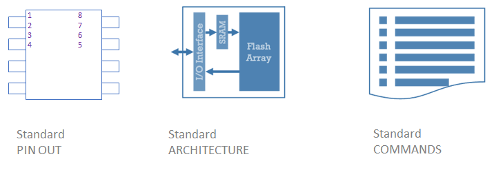
- 8-lead SOIC (150-mil and 208-mil)
- 8-pad Ultra-Thin DFN (5mm x 6mm x 0.6mm)
- Die in Wafer Form
Comparison
Applications
Design & Development
Models
ECAD Models
Schematic symbols, PCB footprints, and 3D CAD models from SamacSys can be found by clicking on the CAD Model links in the Product Options table. If a symbol or model isn't available, it can be requested directly from SamacSys.

Product Options
Applied Filters: