As the workhorse of semiconductor memory, DRAM holds a unique place in the industry thanks to its large storage capacity and ability to feed data and program code to the host processor quickly.
Lately, this unsung hero of the circuit board has been taking a backseat to its logic counterparts, as a wave of high-performance FPGAs, CPUs, GPUs, TPUs and custom accelerator ASICs emerges to meet the massive data processing demands of predictive and generative AI applications. The sheer compute density of these rapidly emerging AI accelerators is shattering even the most ambitious expectations, and the number of processor cores inside data center servers continues to balloon.
However, such explosive growth has had consequences, given that advanced logic scaling continues to outpace DRAM scaling. This gap contributes to a widening performance mismatch between the two that threatens to compromise server performance by forcing high-speed (and costly) processors to waste compute cycles while waiting for main memory to catch up.
A New Approach to DRAM Interface Design
Of course, such imbalances are nothing new. The very nature of the classic Von Neumann model specifies the decoupling of the processor and memory, which creates a chokepoint that prevents designers from optimizing every compute cycle. With the industry’s design and manufacturing investment roadmaps more or less wedded to this architectural paradigm for the foreseeable future, we need a new approach to bring processors and memory into closer alignment.
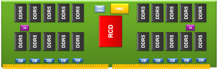
Indeed, DRAM designers are rushing to close the rift, most notably with the introduction of high-speed, high-capacity, third-generation DDR5 DRAM. But more must be done to mesh compute and memory. That was the motivation that drove Renesas to recently launch a registered clock driver (RCD) and client clock driver (CKD) for third-generation DDR5 DRAM servers and client systems across our entire portfolio of memory interfaces for dual inline memory modules (DIMMs), motherboards and embedded applications.
The new DDR5 RCD and DDR5 CKD ICs enable next-generation DIMMs with speeds of up to 6400 and 7200 mega transfers per second (MT/s), respectively, an increase from today’s 5600 MT/s transfer speeds. Renesas’ Gen 3 DDR5 RCD is designed for registered DIMMs (RDIMMs). The CKD is the first in the industry to interface with small-outline DIMMs (SODIMMs), unbuffered DIMMs (UDIMMs), high-performance gaming DIMMs and memory-down applications for client platforms.
Together, these new drivers enable a hierarchy of memories operating at different performance, power and capacity levels. Their adoption is expected to drive the growth of so-called “chiplets,” an emerging form of heterogeneous computing that converges components with different functions, process nodes and electrical characteristics. Heterogeneous computing is also driving research into new approaches to memory and logic within the device and module, inside the server and across the entire server rack.
The Importance of Ecosystem Collaboration
We did not achieve this breakthrough in a vacuum. Working closely with the JEDEC standards body, Renesas is facilitating an ecosystem of development partners and serves as the glue that holds together DRAM and DIMM makers, CPU, GPU and other logic providers, server designers – even hyperscale computing operators like Amazon, Google and Microsoft. In addition to setting a shared roadmap and key performance indicators, the collective ensures design verification and interoperability testing at the device, module and system level – and across all relevant software applications.
The imperative for close collaboration also led us to join the Compute Express Link™ (CXL™) Consortium. The consortium aims to develop open-source standards and technical specifications for data center interconnect. This includes a high-speed memory fabric that achieves performance parity with various forms of compute system architectures.
Ultimately, our goal at Renesas is to empower device, module and system architects to break conventional design constraints. Together, we can unleash the potential of a co-optimized compute-memory architecture and better meet the needs of increasingly sophisticated – and compute-intensive – AI applications.