5P35021 VersaClock 3S Programmable Clock Development Kit
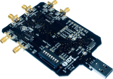
The DEV5P35021 programmable clock development kit is designed to support the 5P35021 VersaClock 3S device. It provides a convenient way of configuring and programming...
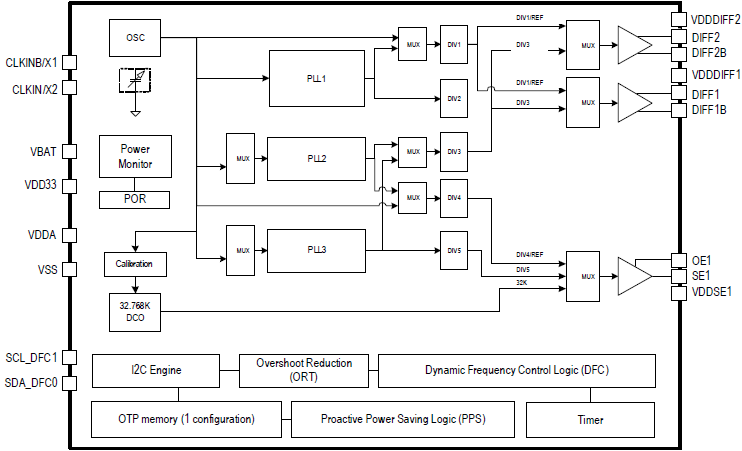
5P35021は、VersaClockプログラマブルクロックジェネレータで、低消費電力、民生、高性能PCI Expressアプリケーション向けに開発されています。 5P35021デバイスは3つのPLLアーキテクチャ設計から成り、各PLLは個別にプログラム可能で、最大5つの周波数出力に対応します。
5P35021は、PPS(Proactive Power Saving)、PPB(Performance-Power Balancing)、ORT(Overshoot Reduction Technology)、超低消費電力DCOなどの独自の機能を内蔵しています。 OTPメモリを内蔵しているため、電源投入の際にプログラミングをせずにデバイスに設定を保存し、その後I²Cインタフェースから再度5P35021をプログラミングすることが可能です。
このデバイスはプログラマブルVCOとPLLソースの選択により、アプリケーションの要件に基づいた電力性能の最適化を可能にします。 また、LVCMOSとLPHCSLに準拠した3つのシングルエンド出力と2組の差動出力をサポートしています。 システムRTCの基準クロックとして、消費電流5μA以下の低消費電力32.768kHzクロックに対応しています。
| Software title
|
Software type
|
会社名
|
|---|---|---|
| Timing Commander Timing Commander™は、Windows™ベースの革新的なソフトウェアプラットフォームで、システム設計を行うエンジニアは、直感的かつ柔軟なグラフィカルユーザインタフェース(GUI)により、高度なタイミングデバイスの構成、プログラミング、モニタリングが行えます。
|
Code Generator | ルネサス |
1件
|
||
The DEV5P35021 programmable clock development kit is designed to support the 5P35021 VersaClock 3S device. It provides a convenient way of configuring and programming...
This is the evaluation board for the Renesas 5P35021 VersaClock 3S programmable clock generator. With RMS phase jitter less than 3 picoseconds over the full 12 kHz to...
[製品選択]テーブル内の製品名をクリックするとSamacSysが提供する回路図シンボル、PCBフットプリント、3D CADモデルがご確認いただけます。 お探しのシンボルやモデルが見つからない場合、Webサイトから直接リクエストできます。

適用されたフィルター
This video introduces IDT's VersaClock 3S Programmable Clock Generators, known for their innovative power-saving features and compact design that eliminates multiple timing components. Designed for applications in consumer, industrial, computing, and automotive sectors, these devices offer low power consumption and low jitter scalability, meeting PCI Express® Gen 1/2/3 standards.
Key features highlighted include Proactive Power Saving, Performance-Power Balancing, Dynamic Frequency Control, and Overshoot Reduction Technology. The video showcases the VersaClock 3S models, including the 5P35023 with multiple outputs and the 5P35021 with a 32.768KHz clock for RTC reference, supported by IDT's Timing Commander software for easy programming.
Related Resources
Transcript
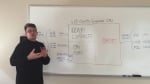
Hi. I'm Nick at the EEWeb Tech Lab and today I have the latest generation of programmable clocks from IDT.
VersaClock® 3S is a family of IDT programmable clocks with innovative features designed specifically for applications requiring low power such as consumer applications and high-performance PCI Express®. VersaClock 3S series has built-in unique features such as Proactive Power Saving, Performance Power Balancing, Overshoot Reduction Technology, and Dynamic Frequency Control.
Proactive Power Saving, or PPS, makes the VersaClock 3S the world's first smart generator with downstream device power mode monitor. By monitoring the status of the downstream device's clock the VersaClock 3S is able to dynamically switch its clock when a downstream device enters sleep mode from a MHz output to a 32 kHz output. This dynamic frequency switching decreases a current of each output clock from 5 or 10 milliamps, depending on the application, down to a tiny 2 microamps.
Performance Power Balancing, or PPB, allows a user to achieve targeted performance while optimizing power consumption. This targeted power mode can be selected using IDT's GUI called the Timing Commander. The Timing Commander GUI is a free download and can be found at idt.com.
IDT's patented Overshoot Reduction Technology affords a smooth frequency transition and keeps a frequency at the targeted frequency. This ORT feature eliminates the overshoot and undershoot common with tradition PLL designs during frequency transitions, which can cause a system to fail.
The user-programmable Dynamic Frequency Control, or DFC, provides a user with up to four preprogrammed frequencies for audio clocks, video clocks, overclocking, or motor speed control. These frequencies can be changed on the fly by using either the hardware pins or the I2C registers.
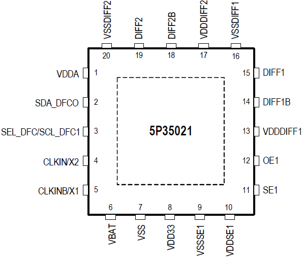
Other device features include multiple function OE pins, the support for two differential clocks and three single-ended clocks, and a built-in watchdog timer.
So let's take a look at some of the IDT products.
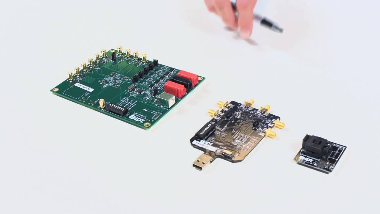
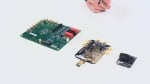
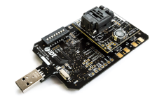
So this is the evaluation board and it's designed for customers who want higher-performance measurements. The IC in the middle, this is the VersaClock 3S. And the USB connector, it accepts 2.0 or 3.0 USB. The mode selector switch is right here. And jumper configurations are here to configure the onboard voltage regulators. A crystal clock is right here for reference on the reference signal. And then the user guide, or the manual, can be downloaded from idt.com.
This is the programming board and it's available for customers who don't need the high-performance of the evaluation board. It accepts both types of socket boards for either the 20 pin or the 24 pin IC. The USB connection, again, is 2.0 or 3.0. It has onboard DC regulatorsthat are actually on the back side. One is here and one is here. And it's compatible with the IDT Timing Commander GUI. And, again, the user guide is downloadable from idt.com.
And this is the socket board. I'll open it up here. There's just a blank part in here right now, but this is where your IC would go. So once you have it in there, then it just connects to this programming board with the sockets, like that. And then you're ready to program.
So this is a Timing Commander GUI. I'm going to start it up. I've downloaded it and I've also downloaded the personality file specific for the VersaClock 3S. I'm loading the file now and the personality file shows up. So these two here. And I'll select this one. Takes just a minute for it to load up.
So the tabs here - there are three. The diagram obviously shows a pinout of the IC. A tab for bit sets that lets you select the bits. And then a tab for registers. It lets you go in and select different register settings.
So if we go back to the diagram pin. This icon here lets you save your settings. This connects to the chip. And this is connection settings here. So the interface or you can change the I2C slave device.
And this is the optimization control for PLLs here. VDD, you can change the voltages. The signal types you can change here. And then the spread-spectrum clocking, you can change these, disable them, or enable them.
IDT's VersaClock 3S family is the industry's most versatile multi-PLL clock generation and crystal consolidation solution for applications including consumer, industrial, communications, medical, automotive, and battery-powered. These devices are offered in small 3x3 or 4x4 QFN packages which makes them ideal for cost-sensitive and dense applications when there's a desire to reduce BOM parts and/or the PCB footprint.
For more information visit idt.com.