Overview
Description
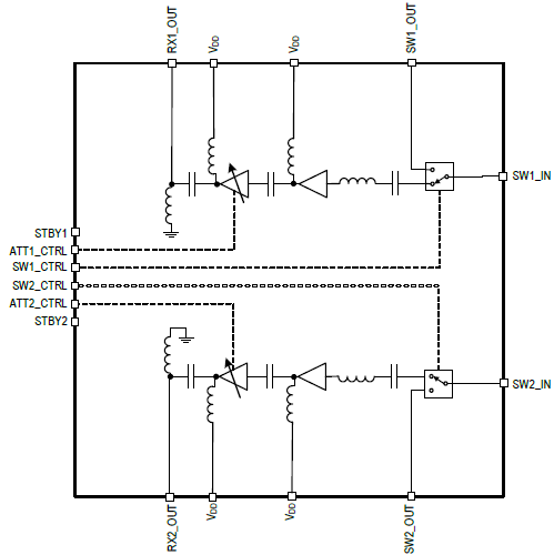
The F0453C is an integrated dual-path RF front-end consisting of an RF switch and two gain stages with 6dB gain control used in the analog front-end receiver of an Active Antenna System (AAS).
The F0453C provides 35dB gain with +23dBm OIP3, +15dBm output P1dB, and 1.35dB noise figure at 3500MHz. Gain is reduced 6dB in a single step with a maximum gain settling time of 31ns. The device uses a single 3.3V supply and 130mA of IDD.
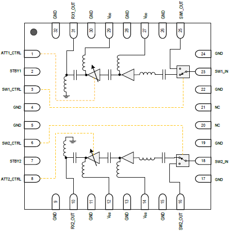
The F0453C is offered in a 6mm × 6mm × 0.8mm, 32-pin LGA package with 50Ω input and output amplifier impedances for ease of integration into the signal path.
Features
- Gain at 3500MHz
- 35dB typical in High Gain Mode
- 29dB typical in Low Gain Mode
- 1.35dB NF at 3500MHz
- +23dBm OIP3 at 3500MHz
- OP1dB at 3500MHz
- +15dBm in High Gain Mode
- +14dBm in Low Gain Mode
- 50Ω single-ended input/output amplifier impedances
- IDD = 130mA
- Independent Standby Mode for power savings
- Supply voltage: +3.15V to +3.45V
- 6mm × 6 mm, 32-pin LGA package
- -40 °C to +105 °C exposed pad operating temperature range
Comparison
Applications
Documentation
Featured Documentation
Log in required to subscribe
|
|
|
|
|---|---|---|
| Type | Title | Date |
| Datasheet | PDF 1.73 MB | |
| Guide | PDF 2.24 MB | |
| End Of Life Notice | PDF 1.11 MB | |
| End Of Life Notice | PDF 1.07 MB | |
| Report | PDF 517 KB | |
| Product Change Notice | PDF 666 KB | |
6 items
|
||
Design & Development
Software & Tools
Boards & Kits

Evaluation
F0453CEVB
Active
Evaluation Board for F0453C RF DVGA
The F0453CEVB is a fully populated test board enabling easy evaluation of the F0453C RF Switch / LNA performance.
Recommended Documents:
Models
ECAD Models
Schematic symbols, PCB footprints, and 3D CAD models from SamacSys can be found by clicking on the CAD Model links in the Product Options table. If a symbol or model isn't available, it can be requested directly from SamacSys.

Product Options
Applied Filters: