概要
説明
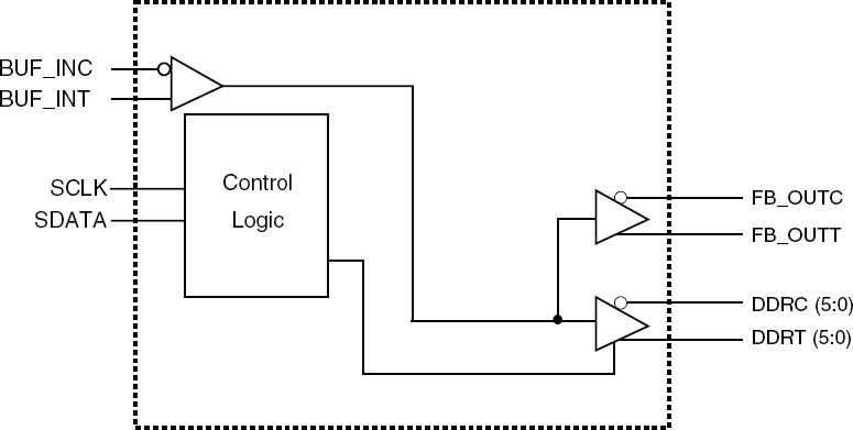
Dual DDR I/II fanout buffer for VIA Chipset
特長
- Low skew, fanout buffer
- SMBus for functional and output control
- Single bank 1-6 differential clock distribution
- 1 pair of differential feedback pins for input to output synchronization
- Supports up to 2 DDR DIMMs
- 266MHz (DDRI 533) output frequency support
- 400MHz (DDRII 800) output frequency support
- Programmable skew through SMBus
- Individual output control programmable through SMBus
- OUTPUT - OUTPUT skew: <100ps
- Output Rise and Fall Time for DDR outputs: 650ps - 950ps
- DUTY CYCLE: 47% - 53%
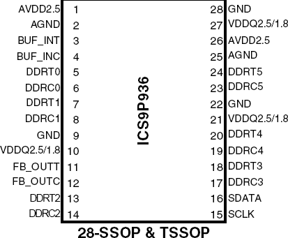
- 28-pin SSOP/TSSOP package
- RoHS compliant packaging
製品比較
アプリケーション
設計・開発
モデル
ECADモデル
SamacSysの回路図シンボル、PCBフットプリント、および3D CADモデルは、製品オプションテーブルのCADモデルリンクをクリックすることで参照できます。シンボルまたはモデルが対応していない場合は、SamacSysに直接リクエスト可能です。

製品選択
適用されたフィルター