概要
説明
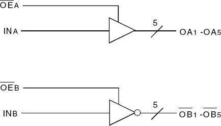
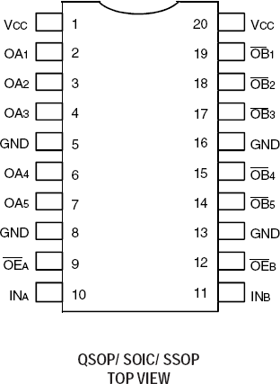
The 74FCT810T is a dual bank inverting/non-inverting clock driver built using advanced dual metal CMOS technology. It consists of two banks of drivers, one inverting and one non-inverting. Each bank drives five output buffers from a standard TTL-compatible input. The FCT810T has a low output skew, pulse skew, and package skew. Inputs are designed with hysteresis circuitry for improved noise immunity. The outputs are designed with TTL output levels and controlled edge rates to reduce signal noise. The part has multiple grounds, minimizing the effects of ground inductance.
特長
- 0.5micron CMOS technology
- Guaranteed low skew < 600ps (max.)
- Very low duty cycle distortion < 700ps (max.)
- Low CMOS levels
- TTL-compatible inputs and outputs
- TTL level output voltage swings
- High drive: -32mA IOH, +48mA IOL
- Two independent output banks with 3-state control: – One 1:5 inverting bank – One 1:5 non-inverting bank
- Available in QSOP, SSOP, and SOIC packages
製品比較
アプリケーション
設計・開発
モデル
ECADモデル
SamacSysの回路図シンボル、PCBフットプリント、および3D CADモデルは、製品オプションテーブルのCADモデルリンクをクリックすることで参照できます。シンボルまたはモデルが対応していない場合は、SamacSysに直接リクエスト可能です。

製品選択
適用されたフィルター


