Overview
Description
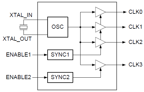
The 5P83904 is a high-performance, 1-to-4 crystal input to LVCMOS fanout buffer with output enable pins. This device accepts a fundamental mode crystal from 10MHz to 40MHz and outputs LVCMOS clocks with best-in-class phase noise performance.
The 5P83904 features a synchronous glitch-free Output Enable function to eliminate any intermediate incorrect output clock cycles when enabling or disabling outputs. It comes in standard TSSOP packages or small QFN packages and can operate from 1.8V to 3.3V supplies.
Features
- Four copies of LVCMOS output clocks with best-in-class phase noise performance
- Phase noise:
Offset noise power (3.3V)- 100Hz: -131dBc/Hz
- 1KHz: -145dBc/Hz
- 10KHz: -154dBc/Hz
- 100KHz: -161dBc/Hz
- Operating power supply modes:
- Full 3.3V, 2.5V, 1.8V
- Mixed 3.3V core/2.5V output operating supply
- Mixed 3.3V core/1.8 V output operating supply
- Mixed 2.5V core/1.8 V output operating supply
- Crystal oscillator interface
- Synchronous Output Enable
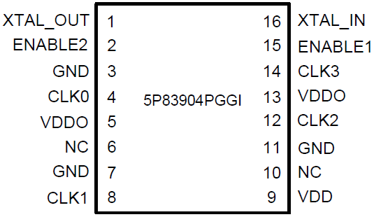
- Packaged in 16-pin TSSOP and QFN packages
- Extended temperature range (-40 °C to +105 °C)
Comparison
Applications
Documentation
Featured Documentation
Log in required to subscribe
|
|
|
|
|---|---|---|
| Type | Title | Date |
| Datasheet | PDF 459 KB | |
| Application Note | PDF 187 KB | |
| Overview | PDF 217 KB | |
| Product Change Notice | PDF 268 KB | |
| Overview | PDF 252 KB | |
| Application Note | PDF 495 KB | |
| Application Note | PDF 442 KB | |
| Application Note | PDF 565 KB | |
8 items
|
||
Design & Development

Product Options
Applied Filters:
Videos & Training
5PB11xx Ultra Low Jitter LVCMOS Buffers
This video provides an overview of the LVCMOS High Performance Clock Buffer Family, highlighting their key features and capabilities.
Related Resources

Video List
News & Blog Posts
News
Mar 24, 2015
|