About This Video
An overview of IDT's full-featured PCI Express (PCIe) clock multiplexers addressing PCIe Gen 1, Gen 2, Gen 3, and Gen 4.
Presented by Ron Wade, PCI Express clock expert at IDT.
Transcript
Hi, this is Ron Wade with IDT. Welcome back to our multi-part series on full-featured PCIe clocks. This particular presentation is part four of five covering clock multiplexers.
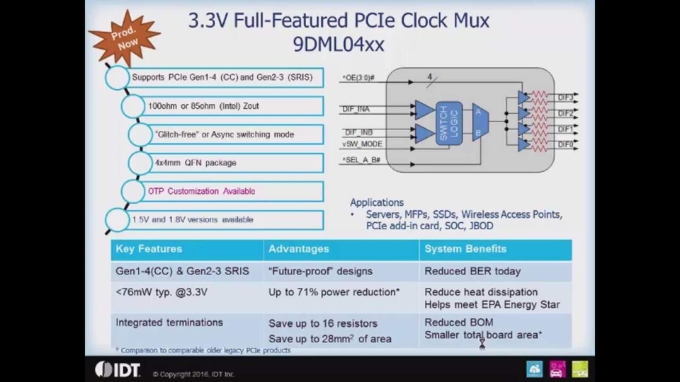
So the 3.3-volt Full-Featured PCIe Clock Mux is the 9DML04 and it supports all of the proposed upcoming PCIe clock standards which include Gen 4 common clocking and Gen 2-3 SRIS.
It has integrated terminations for either 100-ohm environments or 85-ohm environments, so you never need to add a termination resistor. It has two switching modes which I'll come back to in a second. It's packaged in a 4x4 QFN and with this 3.3-volt device, we can factory OTP customize the part for you. For instance, maybe you want a different slew rate or a different output amplitude, or you want your output enabled to be active high instead of active low. These are all configurable.
They also have 1.5 and 1.8-volt parts in the family as well. So the 3.3-volt device… Again, all the muxes have two switching modes. One is called glitch-free, and the other one is called asynchronous. Glitch-free is not a hit-less switch mode, but it is a glitch-free mode. And what we mean by that is you will have an output running on one of the clocks and when you are in glitch-free mode, you switch to the other input. The output will stop so the currently selected clock will stop. There will be a gap of two or three clocks and then the new clock will start up. So that is what we mean by glitch-free switching. No runt pulses, no slivers of clocks. But you will have a little gap in the output as the part internally switches over and synchronizes.
The asynchronous mode is for those cases where you only have one input clock at a time present, and/or you have a strapping mode where if the clock…if the board is plugged into one place, you use clock A, if it's plugged into another place, you use clock B. In that case, you want to use the asynchronous switching mode.
So the 76 mW at 3.3 volts is significantly lower than our legacy parts. The integrated termination save you 16 resistors on your BOM and 28 mm2 of board area. And then with the compatibility with the future PCIe specifications, you can do this design with this part and amortize it over multiple generations of your system.
So the clock multiplexer is basically... All of them have two inputs. And then in the DML04 family, for instance, we have four outputs, and at the 1.5 and 1.8-volt levels, there are one output parts. So 2 and 1 out for the DMV and DMU devices in a 3x3 QFN. And then the four output devices are available at all three voltages in the family, four outputs in a 4x4 QFN and again the 3.3-volt parts Gen 1 through 4 compliant. We're looking at that compliancy for the 1.5 and 1.8-volt parts just as we are looking at the SRnS and SRIS compliancy for those devices.
Pin compatibility across the three members of the family; three operating voltages for the four output and at the two output as well.
So why would you use a four output DML04 as opposed to a 557-06 or 5V41067 which are IDT's legacy parts? Well, performance is one thing. You've got virtually no additive jitter to the PCIe specifications. You've got a roughly 64 - mm2area down to 36 mm2 of area so you're saving almost half the board space. No termination resistors and you're going from 264 milliwatts to 76.
So to summarize that, that's up to 500% lower phase jitter, additive phase jitter here, 58% less area, up to 75% less power, 16 resistors get taken off the BOM The 1.8 volt and 1.5 volt parts can actually save even more power if that is more concern to your system. So really, go for the new parts.
So thank you. That concludes part four of this five-part series.