Overview
Description
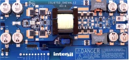
The ISL6752/54EVAL1Z is a new design based on the ISL6752EVAL1Z but with several design modifications to improve the efficiency from 90% to 95%. The control circuit has been moved off the main board onto a daughter card. Two different daughter cards are provided: one using the ISL6752 and the other using the ISL6754. Both control cards utilize the Renesas zero voltage switching (ZVS) topology. The ISL6752 daughter card features pulse by pulse current limiting, and the ISL6754 daughter card features a patented method for average current limiting that results in a brick-wall current limit profile.
The PCB layout of the ISL6752/54EVAL1Z has also been greatly improved over the ISL6752EVAL1Z. Even though the overall size of the board has been reduced, the copper losses have been reduced.
In addition to the ZVS function, this board also incorporates N-Channel FETs as secondary side rectifiers, also known as synchronous rectifiers (SR). Power dissipation of the secondary side rectifiers is reduced because the conduction losses of SRs are significantly less than the conduction losses of PN or Schottky diodes.
Features
- Absolute maximum input voltage 450VDC
- Operating input voltage 350V to 450VDCC
- Maximum input current 2.5ADC
- Rated output current 50ADC
- Current limit 60A ± 5%
- Output voltage 12V ± 5%
- Efficiency at 100% (50A) load 95%
- Efficiency at 20% (10A) load 92%
Applications
Documentation
|
|
|
|
|---|---|---|
| Type | Title | Date |
| Manual - Development Tools | PDF 3.45 MB | |
| Datasheet | PDF 1.02 MB | |
| Datasheet | PDF 1.43 MB | |
3 items
|
||
Product Options
Applied Filters:
