Overview

Description

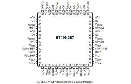
The 8T49N287 has two fractional feedback PLL’s that can be used as a frequency translators with jitter attenuation or a frequency synthesizers. It is equipped with six integer and two fractional output dividers, allowing the generation of up to eight different output frequencies, ranging from 8 kHz to 1 GHz. Output frequencies can be completely independent of the input frequencies, and up to four of these frequencies can be completely independent of each other. The eight outputs may select among LVPECL, LVDS, HCSL or LVCMOS output levels.

The 8T49N287 is ideal for use in a wide range of equipment, including 10G/40G/100G SONET/SDH and Ethernet network line cards, wireless base station baseband units, broadcast video, carrier Ethernet switches, OTN, or on test and measurement applications. The 8T49N287 can be used in GbE/10GbE/100GbE Synchronous Ethernet line card applications in order to preserve the G.8262 compliance from the Synchronous Equipment Timing Source (SETS) on the timing card.

Renesas’ third generation Universal Frequency Translator family also includes the 8T49N285 (2-in / 1-PLL / 8-out), 8T49N286 (4-in / 2-PLL / 8-out), and the 8T49N242 (2-in / 1-PLL / 4-out). These devices are complemented by the 82P33714 and 82P33731 synchronous equipment timing source (SETS) for Synchronous Ethernet (SyncE) and 10G-40G SyncE, respectively.

To see other devices in this product family, visit the Universal Frequency Translators page.

Features

  • Supports GR.1244 Stratum 3 stability in holdover mode
  • Compliant with the requirements outlined in Telcordia GR-253-CORE (SONET) & ITU-T G.813/G.8262 (SDH/SONET & SyncE) when paired with a Synchronous Equipment Timing Source (SETS ) device
  • Generates up to 8 LVPECL / LVDS/HCSL or 16 LVCMOS output clocks ranging from 8kHz up to 1.0 GHz (diff), 8 kHz to 250 MHz (LVCMOS), that meet jitter limits for 10G up to 100G Ethernet and STM-256/OC-768 applications
    • 0.3ps RMS (including spurs), 12 kHz to 20 MHz
  • Accepts up to two LVPECL, LVDS, LVHSTL, HCSL or LVCMOS input clocks ranging from 8 kHz up to 875 MHz
    • Auto and manual input clock selection with hitless switching
    • Clock input monitoring, including support for gapped clocks
  • Phase-Slope Limiting and Fully Hitless Switching options to control output phase transients
  • Operates from a 10 MHz to 40 MHz fundamental-mode crystal
  • Register programmable through I2C / SPI or via external I2C EEPROM
  • 8T49N287-993 “Boot from EEPROM”
  • 8T49N287-994 “powers up disabled”
  • Supported by Timing Commander Software

Comparison

Applications

Documentation

Design & Development

Software & Tools

Software & Tools

Software title
Software type
Company
Timing Commander
Timing Commander™ is an innovative Windows™-based software platform enabling system design engineers to configure, program, and monitor sophisticated timing devices with an intuitive and flexible graphical user interface (GUI).
Code Generator Renesas
1 item

Software Downloads

Type Title Date
Software & Tools - Software Log in to Download ZIP 18.02 MB
Software & Tools - Other Log in to Download ZIP 7.01 MB
2 items

Boards & Kits

Boards & Kits

Models

Videos & Training

UFT Programmable Clock Synthesizer for 100 GbE and OTN Line Cards

Description

Overview of IDT's third generation Universal Frequency Translator (UFT) family of timing devices for high-performance optical networks, wireless base stations, and 100 Gigabit Ethernet (GbE) interface applications. The new UFT devices are the industry's only single-chip programmable solutions capable of generating eight different output frequencies with less than 300 femtoseconds RMS phase jitter over the standard 12 kHz to 20 MHz integration range.
 
The IDT 8T49N28x UFT family of timing devices offers eight independently programmable clocking outputs with the flexibility to apply virtually any input frequency and select virtually any output frequency. The devices' high level of integration and low jitter eliminates the need for separate frequency translation, redundancy management, and jitter attenuation devices -- empowering system designers to save cost and board area by consolidating those functions into a single device. In addition, the device offers significant flexibility in configuration and ease of programmability with IDT's Timing Commander software, making it useful in a variety of sockets and modes of operation with minimal design effort.
 
Presented by Ian Dobson, Director of System Architecture at IDT. Visit the Universal Frequency Translators page for information.


Transcript

Hello, my name is Ian Dobson, I'm the director of System Architecture within our Timing and Synchronization Division here at IDT, and I'm here to talk to you about the third generation of our programmable universal frequency translators. As you can see from the part numbers, there are three members of this family at the time of this recording. There will probably be more by the time you are looking at this. 
 
Our third generation is extending our universal frequency translator family that's been out there solving problems for customers for over three years now. One of the hallmarks of the family is that it takes any input frequency and generates one or more independent output frequencies that are unrelated to that input frequency. Within the family, we have devices that support one, two, three, or four PLL's within a single package. The devices are all extremely flexible and programmable and can be used as frequency synthesizers that accept their input from a low-cost, readily-available quartz crystal, or they can also act as a frequency translator or jitter attenuator, accepting up to four input reference clocks, that can be anywhere, in this third generation, from 8 kHz all the way up to 875 MHz. The family has a number of benefits. Fully programmable, and can be re-used in many different applications and different markets. There are up to four input reference clocks. These clocks support automatic hit-list switching to enable redundancy and system availability. There are multiple options within this family that allows the device to power up without any complex user programming and run straight from power-up. In our third generation family, we've added a new mode to that that allows us to support customer programming via an external e-prong, much as you do for your FPGA's. And of course, one of the main attractions on the device is it supports extremely low RMS jitter on all of its outputs, for any of those demanding applications out there.
 
At IDT, we recognize over the last few years the clock tree has become much more complex in many of the designs out there. But our emphasis is that we want to solve these complex clocking problems simply. So with our third generation of the UFT, we're providing a highly flexible device that will allow the support for multiple different configurations, multiple applications, and multiple different markets within a single device. The high integration that you see on our 282 device in the block diagram here, there are multiple functions that are combined within a single, small package. We're able to generate high-performance clocks from independent sources, like fundamental mode crystals, with RMS jitter less than 0.3 picoseconds. And with our IDT Timing Commander software, we've now made programming of a complex, flexible device like this very simple. This device was originally developed with communications line cards applications in mind. However, we have seen this device and its predecessors used in many different applications across many different market spaces, including some of the example applications listed here. 
 
Of course, one of the key features of the device is that it's able to generate high-performance clocks. We're able to generate clocks that can serve as references for the high-speed FIS, switches, and other demanding applications that are out there today, clocks that have less than 0.3 picoseconds of RMS jitter. These output frequencies can be synthesized using an inexpensive, fundamental mode crystal, a crystal running anywhere from 10 MHz to 40 MHz and generating outputs that are completely independent of that crystal frequency, allowing the use of crystal that's already on your approved parts list. The output frequencies can also be synthesized for any one of up to four input references per PLL. These input references can be very high jitter or maybe even gapped input clocks, such as you see in the OTN space, and still generate that level of performance on the output. One of the things we're particularly excited about with our third generation of the UFT family is a breakthrough fractional output divider technology that we're using within the device. A fractional output divider allows the output clock to be independent from the frequency of the PLL and we can now do that with less than 0.7 picoseconds of RMS jitter, even in that very flexible mode of operation. 
 
So speaking of flexibility, the same device can be used in many different configurations, many applications, we're able to generate outputs with or without input references, we're able to support reliable, redundant operation within the system, we have independent input monitors on each of the inputs, and can support flexible switch-over and hold-over capabilities on a per-PLL basis. The support for gapped clocks allows the device to inter-operate with OTN mappers and FIS, as well as supporting the often complex frequency translations needed in the OTN space. The loop bandwidth of the device is programmable. This allows, via simple register adjustment, to change the loop bandwidth of the device without need for changing any of the external components outside of the device. As you can see from our Timing Commander screenshot here, from our software configuration tool, there are many different signal paths throughout the device. And using this tool, a user is able to simply set up however they want to be able to configure the device for their particular application. There are independent dividers on each output. This allows up to eight different frequencies to be generated from a single device. The device will configure itself from power out, so you can be providing output clocks at the frequency you need in your configuration before your software is even loaded or running. And of course, any functions that you don't end up using can be turned off to save power.
 
The advantage of a highly integrated and flexible device like this… one additional advantage, I should say, is that there is a reduced footprint on your PCB for this clock tree. We're able to generate high-performance clocks from any input frequency. This eliminates the need for a separation of frequency translators on the board and jitter attenuators; those can be combined into a single device generating the desired frequency and performance. As you can see from the block diagram, we're able to support the receive and transmit paths of a communications line card within a single device, because it has two PLL's within it. Additionally, our fractional divider output technology, of which there are two within the devices, allow further independent frequencies to be generated, for a total of eight different output frequencies within a single device. The device architecture supports a digital PLL driving an analog PLL. This provides both flexibility and performance, and the use of the digital PLL will eliminate many external, passive components that may otherwise have been needed, reducing the footprint. Each of the outputs on the device is independently programmable. The output protocols can be selected from one of a large list and the voltages can also be driven independently for each of those outputs. This eliminates the need for external buffers in your system.
 
So I just want to finish off here by saying we have a wide-range of support tools for this product, including the Timing Commander software, and those can be accessed at the URL listed below. I look forward to working with you and helping you solve your complex clocking problems, simply. www.idt.com/go/UFT, www.idt.com/go/sales
 

News & Blog Posts