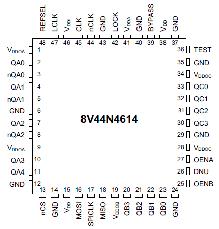
| Lead Count (#) | 48 |
| Pkg. Code | NLG48 |
| Pitch (mm) | 0.5 |
| Pkg. Type | VFQFPN |
| Pkg. Dimensions (mm) | 7.0 x 7.0 x 0.9 |
| Moisture Sensitivity Level (MSL) | 3 |
| Pb (Lead) Free | Yes |
| ECCN (US) | NLR |
| HTS (US) | 8542390001 |
| Lead Count (#) | 48 |
| Carrier Type | Reel |
| Moisture Sensitivity Level (MSL) | 3 |
| Qty. per Reel (#) | 2000 |
| Qty. per Carrier (#) | 0 |
| Pb (Lead) Free | Yes |
| Pb Free Category | e3 Sn |
| Temp. Range | -40 to +85°C |
| C-C Jitter Max P-P (ps) | 20 |
| C-C Jitter Typ P-P (ps) | 10 |
| Core Voltage (V) | 3.3 |
| Feedback Input | No |
| Input Freq (KHz) | 25 - 200 |
| Input Freq (MHz) | 25 - 25, 50 - 50, 100 - 100, 200 - 200 |
| Input Type | Crystal, LVCMOS, LVDS, LVPECL |
| Inputs (#) | 2 |
| Length (mm) | 7 |
| MOQ | 2000 |
| Output Banks (#) | 3 |
| Output Freq Range (KHz) | 25 - 156.25 |
| Output Freq Range (MHz) | 25 - 25, 100 - 100, 125 - 125, 156 - 156 |
| Output Skew (ps) | 50 |
| Output Type | LVDS, LVPECL, LVCMOS |
| Output Voltage (V) | 3.3 |
| Outputs (#) | 13 |
| Package Area (mm²) | 49.0 |
| Phase Jitter Max RMS (ps) | 0.542 |
| Phase Jitter Typ RMS (ps) | 0.395 |
| Pitch (mm) | 0.5 |
| Pkg. Dimensions (mm) | 7.0 x 7.0 x 0.9 |
| Pkg. Type | VFQFPN |
| Prog. Clock | Yes |
| Prog. Interface | SPI |
| Reel Size (in) | 13 |
| Reference Output | No |
| Requires Terms and Conditions | Does not require acceptance of Terms and Conditions |
| Spread Spectrum | No |
| Tape & Reel | Yes |
| Thickness (mm) | 0.9 |
| Width (mm) | 7 |
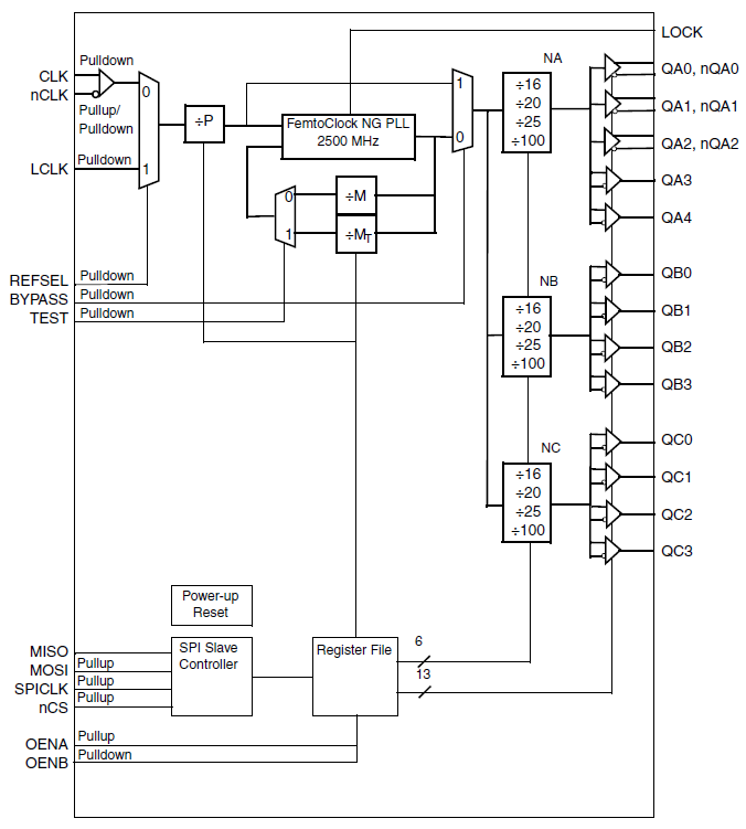
The 8V44N4614 is a FemtoClock® NG clock generator. The device has been designed for frequency generation in high-performance systems such as wireless baseband boards, for instance, to drive the reference clock inputs of processors, PHY, switches, and SerDes devices. The device is very flexible in frequency programming. It allows for the generation of clock frequencies of 156.25MHz, 125MHz, 100MHz, and 25MHz individually at three output banks. One output bank supports configurable LVDS and LVPECL, and the other two output banks support LVCMOS output levels. All outputs are synchronized on the incident rising edge, regardless of the selected output frequency. Selective single-ended LVCMOS outputs can be configured to invert the output phase, effectively forming differential LVCMOS output pairs for noise reduction. The PLL reference signal is either a 25MHz, 50MHz, 100MHz, or 200MHz differential or single-ended clock.
The device is optimized to deliver excellent period and cycle-to-cycle jitter performance, combined with good phase noise performance, and high power supply noise rejection.
The clock generator is configured through an SPI serial interface. Outputs can be configured to any of the available output frequencies. Two hardware pins are available for selecting pre-set output enable/disable configurations. In each of these pre-set configurations, each output can be enabled/disabled individually. A separate test mode is available for an increase or decrease of the output frequencies in 19.53125ppm steps independent of the input frequency. The device is packaged in a lead-free (RoHS 6) 48-lead VFQFN package. The extended temperature range supports wireless infrastructure, telecommunication, and networking end equipment requirements.