Overview
Description
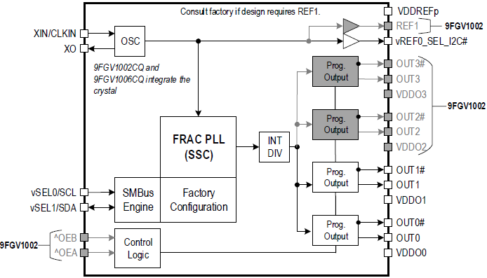
The 9FGV1006 is a member of Renesas' PhiClock™ programmable clock generator family. The 9FGV1006 provides two copies of a single integer, fractional or spread-spectrum output frequency and one copy of the crystal reference input. Two select pins allow for hardware selection of the desired configuration, or two I²C bits all easy software selection of the desired configuration. The user may configure any one of the four OTP configurations as the default when operating in I²C mode. Four unique I²C addresses are available, allowing easy I²C access to multiple components.
Features
- PCIe Gen 1–7 compliant
- PCIe Gen 7 Common Clock jitter < 41fs RMS
- 276fs RMS typical phase jitter at 156.25MHz (12kHz to 20MHz)
- 2 programmable output pairs plus 1 LVCMOS REF output
- 1 integer, fractional or spread-spectrum output frequency per configuration
- 1MHz to 325MHz output frequency (LVDS or LP-HCSL)
- 1MHz to 200MHz output frequency (LVCMOS)
- 1.8V to 3.3V core VDD
- Individual 1.8V, 2.5V, or 3.3V VDDO for each programmable output pair
- Supports HCSL, LVDS, and LVCMOS I/O standards
- Supports AC-coupled LVPECL and CML logic – See AN-891
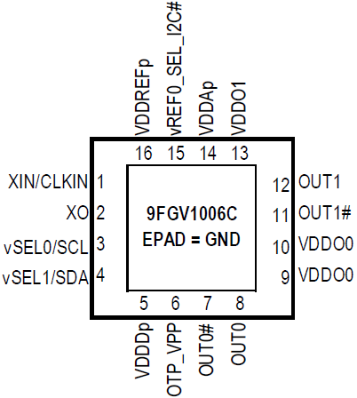
- 3mm × 3mm 16-LGA packages with 50MHz integrated crystal option
- Supported by Timing Commander™ software
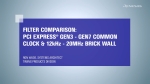
Comparison
Applications
Design & Development
Software & Tools
Boards & Kits
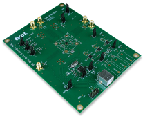
Evaluation Kit for 9FGV1006 Programmable PhiClock™ Generator with Internal 50MHz Crystal
This is the evaluation board for the 9FGV1006Q5 programmable PhiClockTM generator with an internal 50MHz crystal. It provides a convenient way of configuring and...
Featured Documents:
Models
ECAD Models
Schematic symbols, PCB footprints, and 3D CAD models from SamacSys can be found by clicking on products in the Product Options table. If a symbol or model isn't available, it can be requested directly from the website.

Product Options
Applied Filters:
Videos & Training
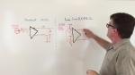
PCIe Reference Clock Jitter Budgets
Ron Wade, chief PCIe system architect explains the fundamental difference in reference clock jitter budgets between the first three generations of the specification and those of Gen4 and Gen5 which raise new challenges for designers.
Related Resources
Video List


News & Blog Posts
| Solving Common Issues with Respect to PCIe Timing Design on the Modern Server System | Blog Post | Apr 14, 2022 |
| Faster Timing Design and Accurate Performance Testing with Jitter Measurement Utility | Blog Post | Jun 15, 2019 |
| Comparing and Contrasting PCIe and Ethernet Clock Jitter Specifications | Blog Post | May 22, 2018 |
| IDT Extends Leadership in Datacenter and Networking Systems with Launch of Its Latest PCI Express Timing Devices | News | Apr 30, 2018 |