Overview
Description
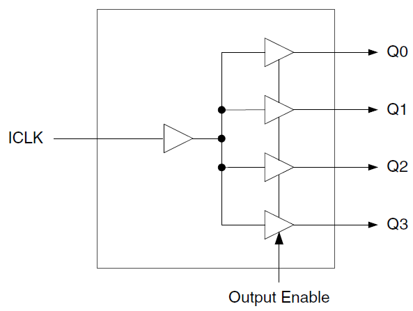
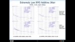
The 553S is a low skew, single input to four output, LVCMOS clock buffer that offers a best-in-class additive phase jitter of sub 50fs.
Features
- Low additive phase jitter RMS: 50fs
- Extremely low skew outputs (50ps)
- Low-cost clock buffer
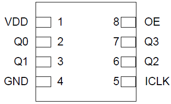
- Packaged in 8-pin SOIC and small 8-pin DFN packages, Pb-free
- Input/Output clock frequency up to 200MHz
- Ideal for networking clocks
- Operating voltages: 1.8V to 3.3V
- Output Enable mode tri-state outputs
- Advanced, low-power CMOS process
- Extended temperature range: -40 °C to +105 °C
Comparison
Applications
Documentation
Featured Documentation
Log in required to subscribe
|
|
|
|
|---|---|---|
| Type | Title | Date |
| Datasheet | PDF 316 KB | |
| Application Note | PDF 187 KB | |
| Overview | PDF 217 KB | |
| Product Change Notice | PDF 268 KB | |
| Product Change Notice | PDF 611 KB | |
| Product Change Notice | PDF 611 KB | |
| Application Note | PDF 495 KB | |
| Application Note | PDF 442 KB | |
| Application Note | PDF 565 KB | |
9 items
|
||
Design & Development
Models
ECAD Models
Schematic symbols, PCB footprints, and 3D CAD models from SamacSys can be found by clicking on products in the Product Options table. If a symbol or model isn't available, it can be requested directly from the website.

Product Options
Applied Filters:
Videos & Training
Low-jitter LVCMOS Fanout Clock Buffers by IDT
This video overviews the LVCMOS Fanout Buffers, showcasing their best-in-class performance with extremely low phase jitter, minimal output skew, and low power consumption, along with other competitive features.
Video List
News & Blog Posts
| IDT Introduces Ultra-Low-Jitter Family of LVCMOS Clock Buffers | News | Mar 24, 2015 |