
Automotive original equipment manufacturers (OEMs) have been at the forefront of mobility and advanced driver assistance systems (ADAS), jockeying for a leadership position in this quickly developing field. As these systems advance, with them comes an increase in the number of semiconductor components in the vehicle to support the increased functionality.
This has provided an opportunity for Renesas Electronics to increase its market offerings, allowing them to add to its traditional base microcontroller (MCU) offerings highly integrated system-on-chip (SoC) processors, memory, and of course power management (PMICs).
However, as the industry evolves, the question remains:” How can we standardize the development and design of these components across the industry, such that we can satisfy the risk and confidently claim the part functionally safe?”
Enter the first edition of ISO 26262, which was the automotive industry's attempt at standardizing the development of the components of these large systems to minimize both:
- Systematic risk, errors generated in the design process through a missed requirement cascade, or an incomplete analysis; and
- Random hardware faults specific to the malfunction of the device in question.
For roughly the last decade, automotive OEMs have been relying on Part 5 of this standard to help them address hardware malfunction to establish what the industry considers “safe” design practices. Renesas has adopted similar standards in the development of their products by analyzing our devices with the Failure Mode Effects and Diagnostic Analysis Report (FMEDA), and Dependent Failure Analysis (DFA) and coming up with a strategy to address random hardware faults in the design.
Building upon Part 5 of the standard, and the level of complexity to which automotive systems have ascended, ISO 26262 has expanded its coverage to include Part 11, which focuses on semiconductor components specifically.
To meet this new demand for functional safety and cost, Renesas provides automotive system designers multi-rail, high power, power management devices (PMICs), in addition to our R-Car system-on-chip processors. Which offers both reduced component count, and a high degree of functionality in which to design their systems.
To help automotive designers understand what to look for when shopping PMICs, we’ll overview the analysis Renesas uses to design functional safety into our PMICs. The Renesas power products all adopt a similar architecture that addresses dependent and random hardware failures at both the component level and the system level; such that the next time you find one of our R-Car kits with a Renesas PMIC next to it, you’ll be confident in your choice.
ISO 26262 Analysis Tools
In reading through ISO 26262, the standard suggests three widely accepted analysis tools that help the safety manager lead the design team to an understanding of how to create a functionally safe product. They are:
- The block diagram;
- The failure mode effects and diagnostic analysis (FMEDA); and
- The dependent failure analysis (DFA).
These tools are suggested for their ability to reduce complexity and allow the team performing the analysis to confidently arrive at a functionally safe design. Renesas employs each of these techniques when designing each PMIC to address random hardware faults.
Block Diagram
Reading through ISO 26262's specification, it's very clear that the authors valued one thing: avoiding needless complexity. And, you’ll notice the standard identifies a standard design practice for creating a block diagram:
- Abstract the design to ensure that each block has a dedicated function, eliminating the need for needless (and often confusing) mixing of functions; and
- Allow the conceptual safety analysis to easily understand information flow and determine where mechanisms need to be implemented.
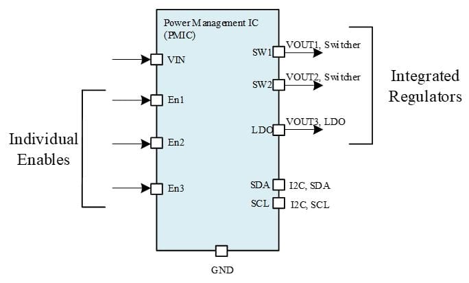
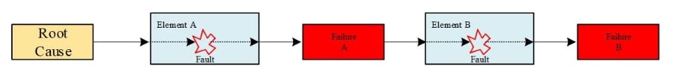
A simple example of such a diagram is shown in Figure 2.
Failure Analysis Tools
Before we start performing the analysis that will lead to design modifications, we need to review the tools that the specification expects us to employ in the analysis. These tools help the design team identify dependencies between safety mechanisms and the elements they protect, and how to apply commonly accepted failure modes in order to come up with a robust design.
- The DFA: This analysis tool is designed to help identify dependent failures, this could take the form of identifying dependencies in the device. For example, those between safety mechanisms and the components they're meant to protect.
Some examples that are often identified from this analysis are:
- VCC: Where drifts, noise, or failures of circuits powering the safety mechanism and the device it powers could adversely impact both.
- Temperature: Where an increase or decrease in temperature could impact a mechanism's monitoring accuracy while at the same time decreasing its ability to control something.
The DFA helps a design to become free from interference by identifying dependencies and mitigating them. Next is the:
- The FMEDA: This analysis tool considers commonly accepted failure modes such as broken resistor strings and component drift to analyze the impact on function. It is also used as a calculator, justifying your safety coverage for an ASIL rating.
While the DFA is used to determine independence to help create a design that is free from dependencies, the FMEDA is implemented as a straightforward approach. The goal of the FMEDA is to go through the hierarchy of the design and apply suggested failure modes to each element. Failures covered here were initially introduced in Part 5 of ISO 26262 and then expanded in Part 11 in the Second Edition. They include:
- Resistor failures and component drift
- Soft error rate in memory, and stuck at faults in digital logic circuits
- Data transmission failures
In the conceptual phase, these faults are applied to the design, mechanisms are created to address the failure modes, and then a coverage is assigned.
Introducing Renesas PMIC Architecture
To understand how Renesas includes the results from these analyses, we’ll first define the major elements of our devices.
- Voltage reference generation: This normally includes the bandgap and any other devices that need a bias.
- Internal rail generation: The internal power domain that provides power to the internal components of the device.
- The switches: This includes the pre-driver and driver circuitry that provide the switching from the input voltage.
- The PWM control circuitry: This comprises the entirety of the control loop.
- Regulator enabling: In general, these are things that enable or disable regulation.
- Digital core: The glue that ties the above together, allowing flexibility to the part such that it can be configured to fit multiple different applications.
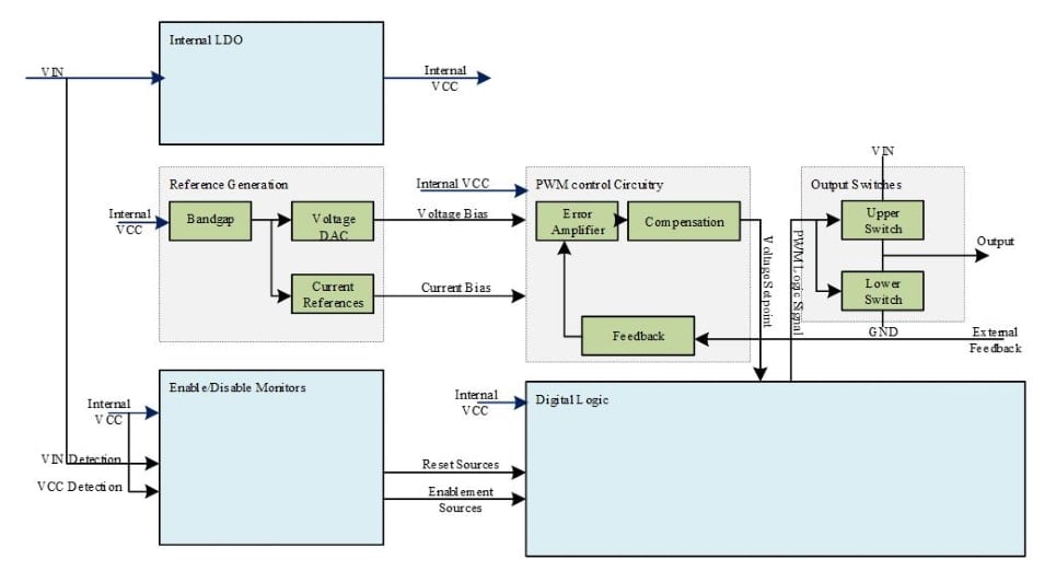
And typically, this is how these systems work to form the basics of a power management device, which is shown in Figure 3; prior to the safety analysis.
Combining the DFA and FMEDA, we can conceptually analyze our architecture and come up with mechanisms and additional architecture enhancements to improve our robustness to hardware failures. While this analysis is not considered to be exhaustive, it will provide some context to our datasheet capabilities.
Internal Rail and Bias Generation
In our hierarchy, we start by creating a powertrain used to help generate bias for all our elements, part of which is a DAC that will provide tap voltages for various references around the device.
We define the fault models from the DFA and come up with the following.
- Common cause faults (CCF): Where a singular fault leads to two faults in two separate elements.
- Cascading faults: Where a fault in one element, leads to a fault in another element.
Taking these two fault models into context against Figure 3, we see that there is only one source of bias and VCC, a failure in that would cascade resulting in a CCF impacting voltage regulation targets and any monitor used to monitor them.
To address this, the original architecture is modified to be more independent.
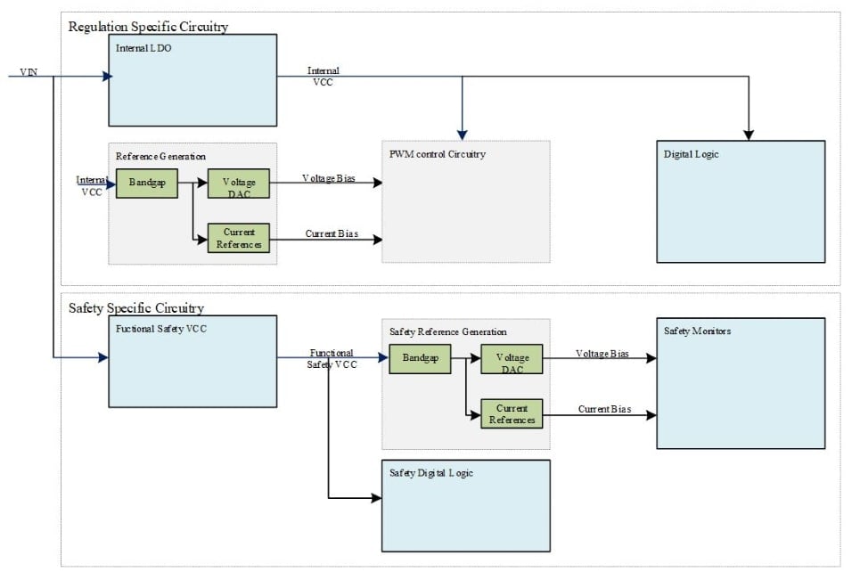
Figure 6 illustrates just one way to address this dependency, in which there are separate bias circuits (bandgaps) and voltage DACs to create separate bias points. This reduces the dependency between circuits and is often why you will find an independent bandgap, bandgap monitor, and VCC monitor on many of our datasheets. The more rigid the safety requirements, the more complex the solution becomes.
PWM Control Circuit & Output Switches and Drivers
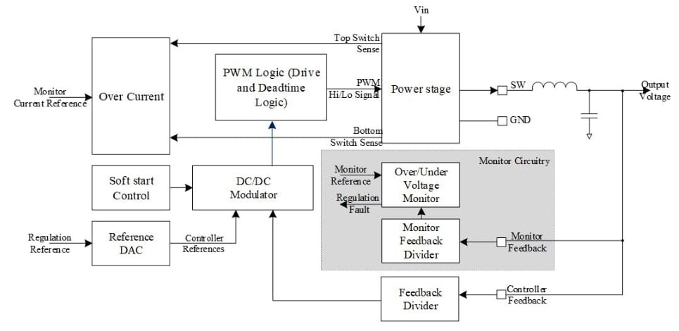
Arguably the most important part of a power management device, the feedback loop design is critical since the choice in architecture denotes what type of safety mechanisms are necessary as well as performance. An example of failure modes analyzed are:
- Failure of the output switches by being stuck high or low: This would lead to an irregularity in switching due to shoot through or directly connecting the output to either ground or VIN.
- Compensation, which damps the response of the control loop to prevent excessive deviations from the setpoint during a load change: A potential failure here could result in an overvoltage event or oscillatory behavior if the bandwidth of the controller drastically changes.
As many failures result in the output voltage deviating from its setpoint or the output current exceeding the safe rating of the device or its loads, the hallmarks of our power management devices are safety mechanisms that monitor the output current and output voltage. These safety mechanisms are often implemented via comparators or onboard analog-to-digital (A/D) converter.
Next, we continue with the DFA and focus on the feedback node. In the feedback path, there is typically a resistor divider network that translates the output voltage to an internal reference level. Loss of that resistor due to a failure will result in the malfunction of the device as the target setpoint becomes incorrect and equally impacts the monitor's ability to catch it.
This leads to the following criteria:
- The device needs to implement two independent sources of feedback to address the dependent failure of the feedback node shorting to another pin or another voltage on the board; and
- This independent source of feedback needs a redundant resistor divider to address the failure mode of any part of the resistor feedback network shorting.
For this reason, you will often see a feedback pin and another pin that is used for monitoring as a part of our devices. If the feedback resistor is instead internal, it is redundant and often through a different path.
For the last two sections, the design turns its focus to things that are often under the category of monitors instead of the control loop.
Monitors and Controls
The monitors and enabling controls are arguably some of the most important circuits in the device as they are essential for the implementation of safety mechanisms that ensure the system is functionally safe. They are comprised of a series of comparator circuits that make up:
- Over-current monitors.
- Power on reset detectors.
- Output voltage (over and undervoltage) monitoring.
- Internal clock monitoring
In conducting the FMEDA, we apply comparator output stuck at faults (stuck high and low). Of these two faults, stuck low is the more impactful as the fault occurrence would be missed in normal operation, representing a latent fault. To increase the device’s ability to detect these stuck low faults, Renesas PMICs implement a self-test (ABIST).
The process is outlined in Figure 8:
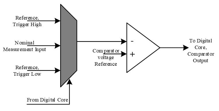
The digital controller switches the inputs to the comparator to force a trigger, and after successful determination, the input control becomes nominal again.
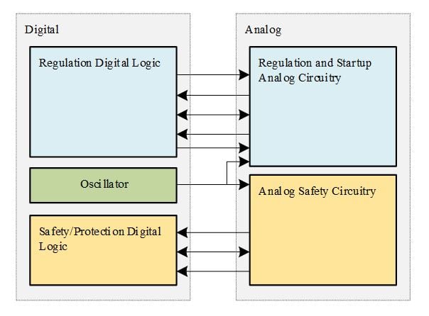
Digital Core
The digital core sits next to the analog parts, as shown in Figure 9, and is often broken up between a section of digital logic that makes functionally safe decisions, and a section responsible for startup and control of the regulator.
This architecture is often preferred to mitigate the possibility of dependencies found through a DFA analysis. To better understand the breakup of the digital core, see Figure 9, where the main functions consist of:
- Configuration, often in terms of runtime configuration registers and one-time programmable (OTP) fuses;
- Functional safety decision making, often realized as a state machine; and
- Communication, either implemented as a I2C or SPI controller.
Here we apply our FMEDA criteria in terms of bit corruption to the one-time programmable (OTP) fuse array and configuration register, resulting in a misconfiguring of the chip; either at startup and during runtime. To protect against this issue, a cyclic redundancy calculation (CRC) is executed both at startup and periodically on the configuration of the device. This is also extended to the communication interface.
While the list of digital safety mechanisms and design options is vast, it is normal to see the following among the top listed safety mechanisms in addition to the CRC:
- Redundant logic where necessary;
- Clock monitoring; and
- Logic BISTing (LBIST) which, like the ABIST, checks the digital logic for critical stuck faults.
Conclusion
With each new design comes a new set of safety mechanisms implemented by the design and safety teams, which the marketing team then uses as saleable features. The conceptual analysis presented in this article is meant to give you, the reader, some tools to understand how we here at Renesas create ASIL-rated power management devices and the reason we have various ‘safety-related' features listed in our hardware datasheet.