Image


The Renesas clock buffer (clock driver) portfolio includes devices with up to 27 outputs. Differential outputs such as LVPECL, LVDS, HCSL, CML, HSTL, as well as selectable outputs, are supported for output frequencies up to 3.2GHz and single-ended LVCMOS outputs for frequencies up to 350MHz. Some buffers are available with mixed output signaling. The Renesas buffer portfolio has devices supporting supply voltages from 1.2V up to 5V and that are available in commercial and industrial temperature ranges. Fanout buffers and clock dividers are general-purpose clock building block devices that can be used in any number of applications. They are ideal for clock and signal distribution in a large variety of systems, from personal computers to consumer electronics or industrial systems, as well as high-performance networking and communications systems.
PCIe
JESD204B
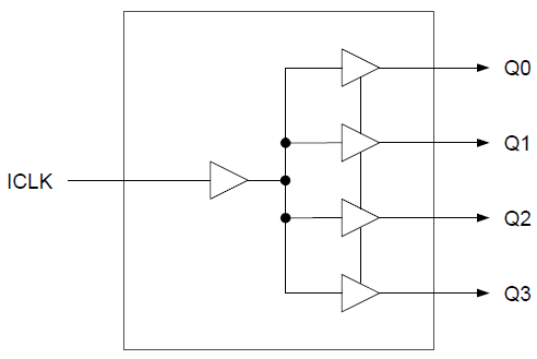
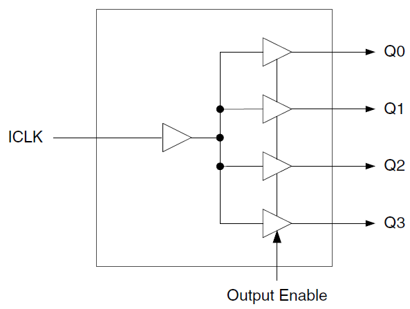
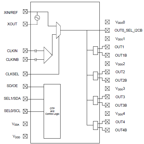
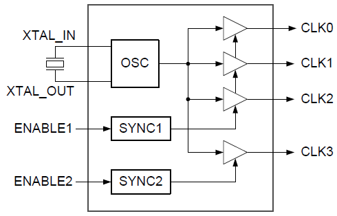
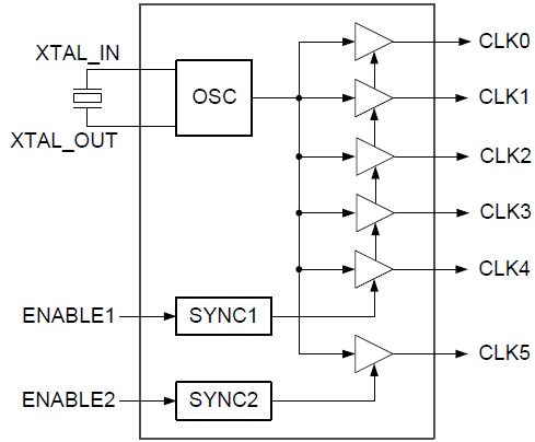
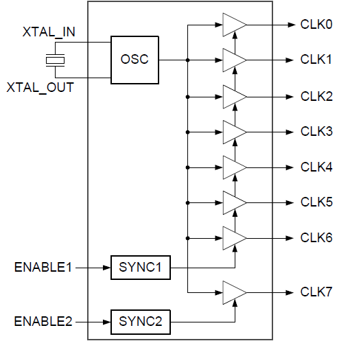
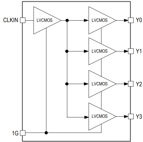
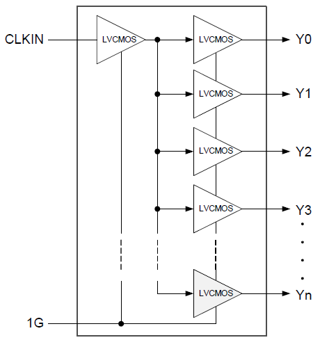
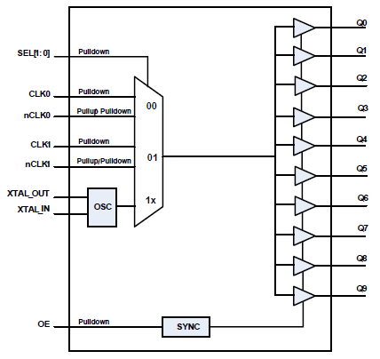
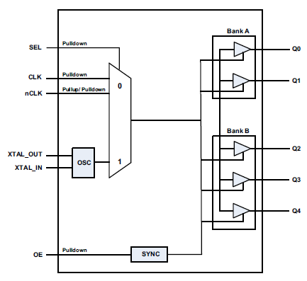
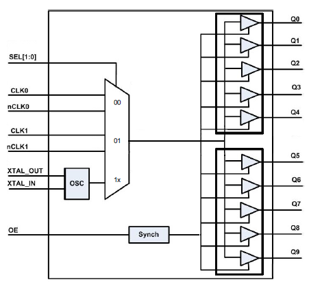
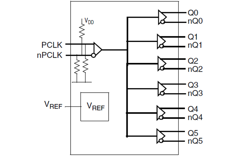
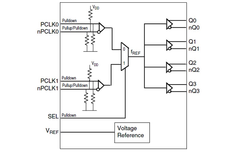
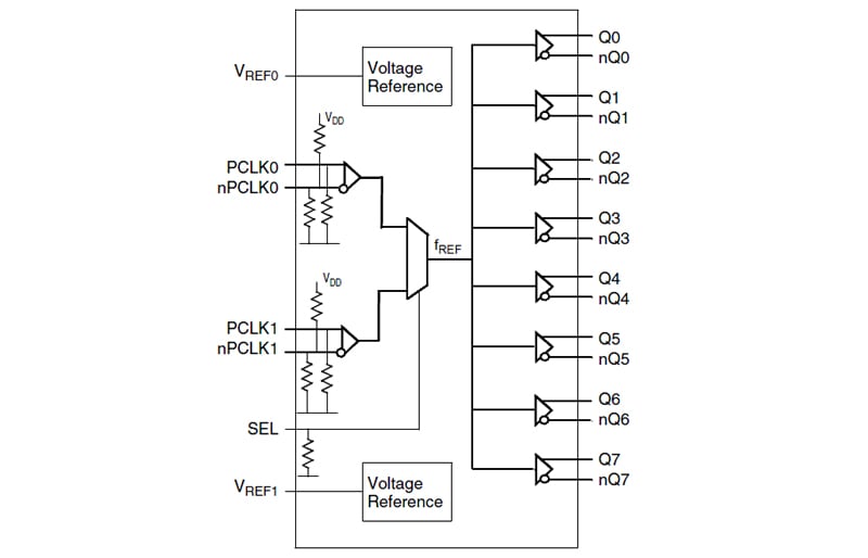
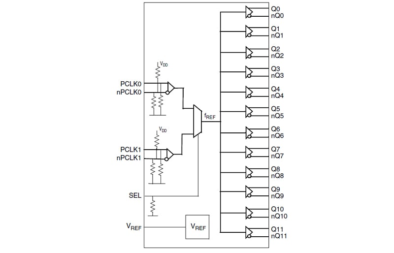
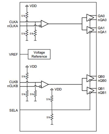
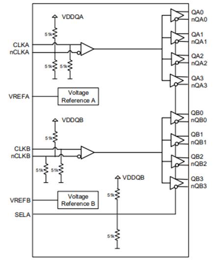
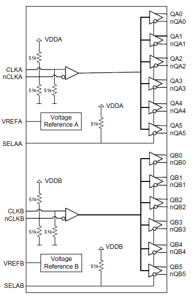
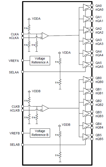
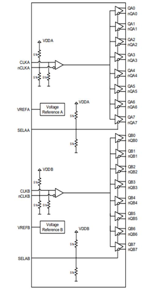
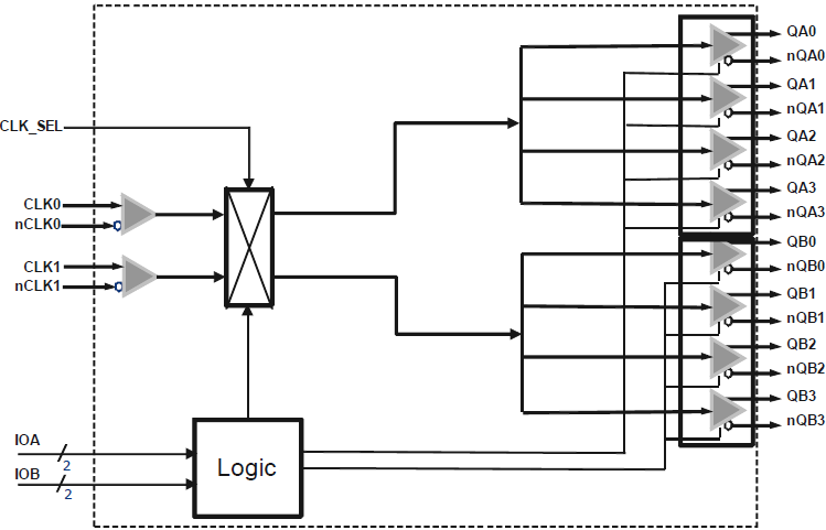
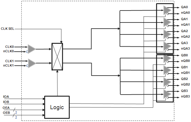
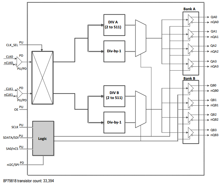
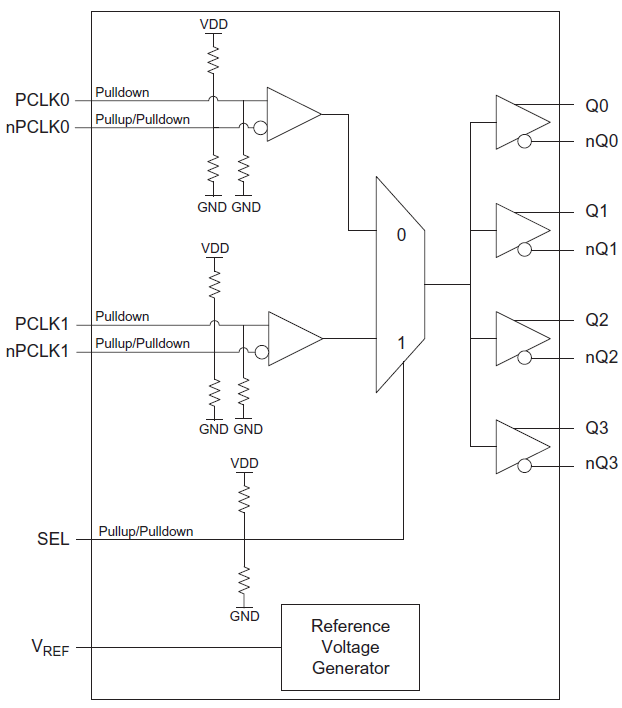
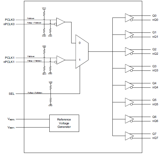
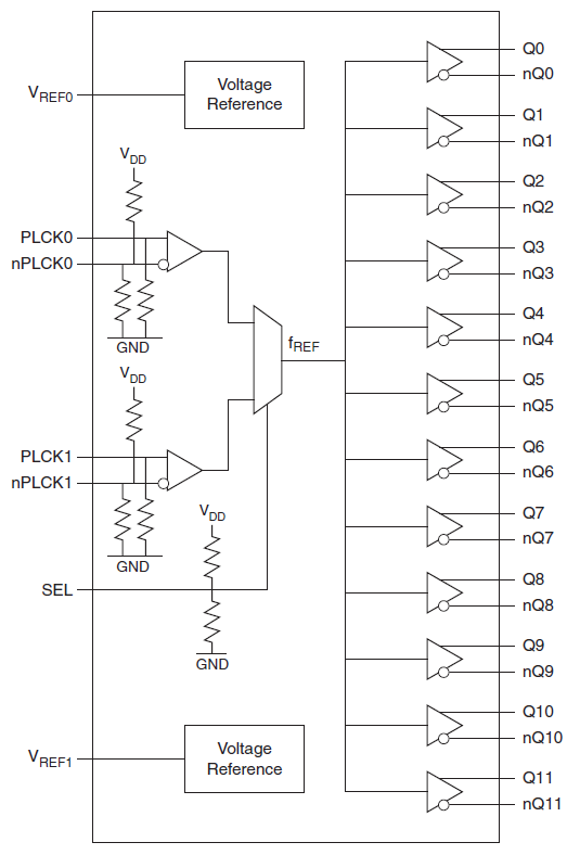
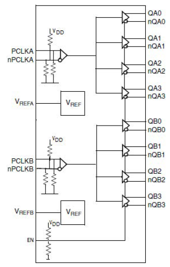
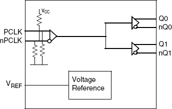
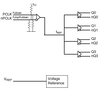
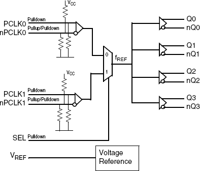
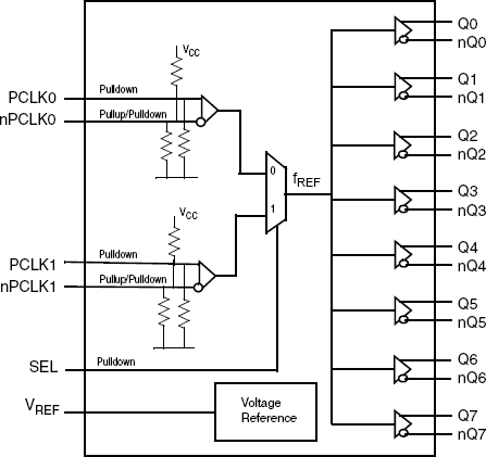
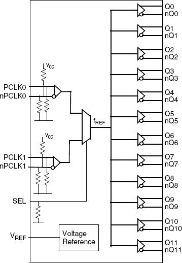
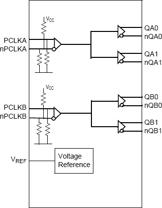
Fanout buffers are a useful building block of many clock trees, providing signal buffering and multiple low-skew copies of the input signal. The clock buffer from a single input reduces loading on the preceding driver and provides an efficient clock distribution network. Single output clock buffers are useful for translating a clock from one signaling standard to another (e.g. LVCMOS-in to LVPECL-out). Some devices have an integrated crystal oscillator, requiring only a low cost external fundamental-mode quartz crystal. The integrated oscillator provides an extremely low phase noise reference clock to drive jitter-sensitive devices such as the clock inputs of PHYs. If the exact buffer configuration is not found in the extensive Renesas fanout buffer offerings, customers may consider devices in the Renesas clock divider or clock multiplexer portfolio that, when used in divide-by-1 mode or proper select mode, can also function as a fanout buffer.
Function |
Outputs (#) |
Output Type |
Output Freq Range (MHz) |
Input Type |
Output Banks (#) |
Output Voltage (V) |
Output Skew (ps) |
Additive Phase Jitter Typ RMS (fs) |
Pkg. Dimensions (mm) |
Pkg. Type |
Prog. Interface |
105°C Max. Case Temp. |
Advanced Features |
|
|---|---|---|---|---|---|---|---|---|---|---|---|---|---|---|
| Part Number | ||||||||||||||
| Low Skew 1 to 4 Clock Buffer | Buffer | 4 | LVCMOS | 0 - 200 | LVCMOS | 1 | 1.8, 2.5, 3.3 | 65 | 35 | 2.0 x 2.0 x 0.5, 4.9 x 3.9 x 1.5 | COL, SOIC | |||
| Low Skew 1 to 4 Clock Buffer | Buffer | 4 | LVCMOS | 0 - 200 | LVCMOS | 1 | 1.8, 2.5, 3.3 | 65 | 35 | 2.0 x 2.0 x 0.5, 4.9 x 3.9 x 1.5 | COL, SOIC | |||
| Programmable Fanout Buffer | Buffer, Multiplexer | 3 | HCSL, LVCMOS, LVDS, LVPECL | 1 - 350 | Crystal, HCSL, LVCMOS, LVDS, LVPECL | 3 | 1.8, 2.5, 3.3 | 35 | 4.0 x 4.0 x 0.9 | VFQFPN | I2C, Pin select | |||
| Programmable Fanout Buffer | Buffer, Multiplexer | 5 | HCSL, LVCMOS, LVDS, LVPECL | 1 - 350 | Crystal, HCSL, LVCMOS, LVDS, LVPECL | 5 | 1.8, 2.5, 3.3 | 35 | 4.0 x 4.0 x 0.9 | VFQFPN | I2C, Pin select | |||
| 1.8 V to 3.3 V 1:4 Crystal Input to LVCMOS Output High-Performance Clock Fanout Buffer with OE | Buffer | 4 | LVCMOS | 0 - 200 | Crystal, LVCMOS | 1 | 1.8, 2.5, 3.3 | 65 | 50 | 2.5 x 2.5 x 0.5, 5.0 x 4.4 x 1.0 | COL, TSSOP | |||
| 1.8 V to 3.3 V 1:6 Crystal Input to LVCMOS Output High-Performance Clock Fanout Buffer with OE | Buffer | 6 | LVCMOS | 0 - 200 | Crystal, LVCMOS | 1 | 1.8, 2.5, 3.3 | 65 | 50 | 2.5 x 2.5 x 0.5, 5.0 x 4.4 x 1.0 | COL, TSSOP | |||
| 1.8 V to 3.3 V 1:8 Crystal Input to LVCMOS Output High-Performance Clock Fanout Buffer with OE | Buffer | 8 | LVCMOS | 0 - 200 | Crystal, LVCMOS | 1 | 1.8, 2.5, 3.3 | 65 | 50 | 3.0 x 3.0 x 1.0, 6.5 x 4.4 x 1.0 | TSSOP, VFQFPN | |||
| 1.8V to 3.3V 1:2 LVCMOS High Performance Clock Buffer | Buffer | 2 | LVCMOS | 0 - 200 | LVCMOS | 1 | 1.8, 2.5, 3.3 | 65 | 35 | 2.0 x 2.0 x 0.5, 3.1 x 4.4 x 1.0 | COL, TSSOP | |||
| 1.8 V to 3.3 V 1:4 LVCMOS High Performance Clock Buffer | Buffer | 4 | LVCMOS | 0 - 200 | LVCMOS | 1 | 1.8, 2.5, 3.3 | 65 | 35 | 2.0 x 2.0 x 0.5, 2.0 x 2.0 x 0.75, 3.1 x 4.4 x 1.0 | COL, TSSOP | |||
| 1.8 V to 3.3 V 1:6 LVCMOS High Performance Clock Buffer | Buffer | 6 | LVCMOS | 0 - 200 | LVCMOS | 1 | 1.8, 2.5, 3.3 | 65 | 35 | 2.5 x 2.5 x 0.5, 5.0 x 4.4 x 1.0 | COL, TSSOP | |||
| 1.8 V to 3.3 V 1:8 LVCMOS High Performance Clock Buffer | Buffer | 8 | LVCMOS | 0 - 200 | LVCMOS | 1 | 1.8, 2.5, 3.3 | 65 | 35 | 2.5 x 2.5 x 0.5, 5.0 x 4.4 x 1.0 | COL, TSSOP | |||
| 1.8 V to 3.3 V 1:10 LVCMOS High Performance Clock Buffer | Buffer | 10 | LVCMOS | 0 - 200 | LVCMOS | 1 | 1.8, 2.5, 3.3 | 65 | 35 | 3.0 x 3.0 x 1.0, 6.5 x 4.4 x 1.0 | TSSOP, VFQFPN | |||
| 1.8 V 1:3 TCXO / LVCMOS High-Performance Clock Buffer | Buffer | 3 | LVCMOS | 0 - 200 | LVCMOS, Sine Wave | 1 | 1.8 | 65 | 50 | 2.0 x 2.0 x 0.75 | DFN | |||
| 1.8 V 1:4 TCXO / LVCMOS High-Performance Clock Buffer | Buffer | 4 | LVCMOS | 0 - 200 | LVCMOS, Sine Wave | 1 | 1.8 | 65 | 50 | 2.5 x 2.5 x 0.5 | COL | |||
| 1.8 V 1:6 TCXO / LVCMOS High-Performance Clock Buffer | Buffer | 6 | LVCMOS | 0 - 200 | LVCMOS, Sine Wave | 1 | 1.8 | 65 | 50 | 3.0 x 3.0 x 1.0 | VFQFPN | |||
| 2.5 V to 3.3 V 1:3 TCXO / LVCMOS High-Performance Clock Buffer | Buffer | 3 | LVCMOS | 0 - 200 | LVCMOS, Sine Wave | 1 | 2.5, 3.3 | 65 | 50 | 2.0 x 2.0 x 0.75 | DFN | |||
| 2.5 V to 3.3 V 1:4 TCXO / LVCMOS High-Performance Clock Buffer | Buffer | 4 | LVCMOS | 0 - 200 | LVCMOS, Sine Wave | 1 | 2.5, 3.3 | 65 | 50 | 2.5 x 2.5 x 0.5 | COL | |||
| 2.5 V to 3.3 V 1:6 TCXO / LVCMOS High-Performance Clock Buffer | Buffer | 6 | LVCMOS | 0 - 200 | LVCMOS, Sine Wave | 1 | 2.5, 3.3 | 65 | 50 | 3.0 x 3.0 x 1.0 | VFQFPN | |||
| Low Skew,1-to-6,Differential-to-2.5V,3.3V LVPECL/ECL Fanout Buffer | Buffer | 6 | LVPECL | 0 - 2000 | CML, LVDS, LVPECL | 1 | 2.5, 3.3 | 50 | 100 | 6.5 x 4.4 x 1.0 | TSSOP | |||
| Low Skew,1-to-2,Differential-to-2.5V,3.3V LVPECL/ECL Fanout Buffer | Buffer | 2 | ECL, LVPECL | 0 - 2500 | CML, LVDS, LVPECL, SSTL | 1 | 2.5, 3.3 | 5 | 26 | 3.0 x 3.0 x 0.97, 4.9 x 3.9 x 1.5 | SOIC, TSSOP | |||
| Low Skew,1-to-5 Differential-to-2.5V,3.3V LVPECL/ECL Fanout Buffer | Buffer, Multiplexer | 5 | LVPECL | 0 - 2000 | CML, LVDS, LVPECL, SSTL | 1 | 2.5, 3.3 | 55 | 100 | 6.5 x 4.4 x 1.0 | TSSOP | |||
| Low Skew, 1-to-10 Differential-to-2.5V, 3.3V LVPECL / ECL Fanout Buffer | Buffer, Multiplexer | 10 | LVPECL | 0 - 2500 | LVDS, LVPECL, SSTL | 1 | 2.5, 3.3 | 50 | 30 | 5.0 x 5.0 x 0.9 | VFQFPN | |||
| Low Skew,1-to-12,Differential-to-3.3V,2.5V LVPECL Fanout Buffer | Buffer | 12 | LVPECL | 0 - 1500 | CML, LVPECL, SSTL | 1 | 2.5, 3.3 | 50 | 60 | 5.0 x 5.0 x 0.9 | VFQFPN | |||
| Crystal or Differential to LVCMOS/ LVTTL Clock Buffer | Buffer, Multiplexer | 10 | LVCMOS | 0 - 200 | Crystal, HCSL, LVCMOS, LVDS, LVPECL | 1 | 1.5, 1.8, 2.5, 3.3 | 63 | 22 | 5.0 x 5.0 x 0.9 | VFQFPN | |||
| Crystal or Differential to LVCMOS/ LVTTL Clock Buffer | Buffer, Multiplexer | 5 | LVCMOS | 0 - 200 | Crystal, HCSL, LVCMOS, LVDS, LVPECL | 2 | 1.5, 1.8, 2.5, 3.3 | 30 | 30 | 4.0 x 4.0 x 0.9 | VFQFPN | |||
| Crystal or Differential to LVCMOS/ LVTTL Clock Buffer | Buffer, Multiplexer | 10 | LVCMOS | 0 - 200 | Crystal, HCSL, LVCMOS, LVDS, LVPECL | 2 | 1.5, 1.8, 2.5, 3.3 | 30 | 30 | 5.0 x 5.0 x 0.9 | VFQFPN | |||
| 1:2 LVDS 1.8V / 2.5V Fanout Buffer for 1PPS and High-Speed Clocks | Buffer | 2 | LVDS | 0 - 1200 | CML, LVDS, LVPECL | 1 | 1.8, 2.5 | 20 | 42 | 3.0 x 3.0 x 1.0 | VFQFPN | |||
| 1:6 LVDS Output 1.8V Fanout Buffer | Buffer | 6 | LVDS | 0 - 1200 | CML, LVDS, LVPECL | 1 | 1.8, 2.5 | 20 | 39 | 4.0 x 4.0 x 1.0 | VFQFPN | |||
| 2:4 LVDS 1.8V / 2.5V Fanout Buffer for 1PPS and High-Speed Clocks | Buffer, Multiplexer | 4 | LVDS | 0 - 1200 | CML, LVDS, LVPECL | 1 | 1.8, 2.5 | 14 | 42 | 3.0 x 3.0 x 1.0 | VFQFPN | |||
| 2:8 LVDS 1.8V / 2.5V Fanout Buffer for 1PPS and High-Speed Clocks | Buffer, Multiplexer | 8 | LVDS | 0 - 1200 | CML, LVDS, LVPECL | 1 | 1.8, 2.5 | 20 | 41 | 5.0 x 5.0 x 0.8 | VFQFPN | |||
| 2:12 LVDS 1.8V / 2.5V Fanout Buffer for 1PPS and High-Speed Clocks | Buffer, Multiplexer | 12 | LVDS | 0 - 1200 | CML, LVDS, LVPECL | 1 | 1.8, 2.5 | 12 | 73 | 6.0 x 6.0 x 0.9 | VFQFPN | |||
| Dual 1:2 LVDS 1.8V / 2.5V Fanout Buffer for 1PPS and High-Speed Clocks | Buffer | 4 | LVDS | 0 - 2000 | LVCMOS, LVDS, LVPECL | 2 | 1.8, 2.5 | 30 | 45 | 3.0 x 3.0 x 1.0 | VFQFPN | Yes | Dual Buffer, Output Amplitude Control | |
| Dual 1:4 LVDS 1.8V / 2.5V Fanout Buffer for 1PPS and High-Speed Clocks | Buffer | 8 | LVDS | 0 - 2000 | LVCMOS, LVDS, LVPECL | 2 | 1.8, 2.5 | 30 | 45 | 5.0 x 5.0 x 0.8 | VFQFPN | Yes | Dual Buffer, Output Amplitude Control | |
| Dual 1:6 LVDS Output 1.8V / 2.5V Fanout Buffer | Buffer | 12 | LVDS | 0 - 2000 | LVCMOS, LVDS, LVPECL | 2 | 1.8, 2.5 | 40 | 45 | 3.59 x 3.04 x 0.6 | WLCSP | Yes | Dual Buffer, Output Amplitude Control | |
| Dual 1:6 LVDS Output 1.8V / 2.5V Fanout Buffer | 1.8, 2.5 | 6.0 x 6.0 x 0.9 | VFQFPN | |||||||||||
| Dual 1:8 LVDS 1.8V / 2.5V Fanout Buffer for 1PPS and High-Speed Clocks | Buffer | 16 | LVDS | 0 - 2000 | LVCMOS, LVDS, LVPECL | 2 | 1.8, 2.5 | 40 | 45 | 7.0 x 7.0 x 0.9 | VFQFPN | Yes | Dual Buffer, Output Amplitude Control | |
| Low Additive Jitter 2:8 Buffer with Universal Differential Outputs | Buffer | 8 | CML, HCSL, LVDS, LVPECL | 0.000001 - 1000 | CSL, LVCMOS, LVDS, LVHSTL, LVPECL | 2 | 1.8, 2.5, 3.3 | 100 | 70 | 5.0 x 5.0 x 0.9 | VFQFPN | Pin select | ||
| Low Additive Jitter 2:8 Buffer with CMOS / Differential Outputs | Buffer, Divider, Multiplexer | 8 | LVCMOS, LVDS, LVPECL | CSL, LVCMOS, LVDS, LVHSTL, LVPECL | 2 | 1.8, 2.5, 3.3 | 100 | 80 | 5.0 x 5.0 x 0.9 | VFQFPN | Pin select | |||
| Programmable Low Additive Jitter 2:8 Buffer with Dividers and Universal Outputs | Buffer, Divider | 8 | CML, HCSL, LVDS, LVPECL | 0.000001 - 700 | LVCMOS, LVDS, LVHSTL, LVPECL | 2 | 1.5, 1.8, 2.5, 3.3 | 100 | 60 | 5.0 x 5.0 x 0.9 | VFQFPN | I2C | ||
| 2:4, LVDS Output Fanout Buffer, 2.5V | Buffer, Multiplexer | 4 | LVDS | 0 - 2000 | LVDS, LVPECL | 1 | 2.5 | 20 | 95 | 3.0 x 3.0 x 1.0 | VFQFPN | |||
| 2:4, LVDS Output Fanout Buffer, 3.3 V | Buffer, Multiplexer | 4 | LVDS | 0 - 2000 | LVDS, LVPECL | 1 | 3.3 | 20 | 95 | 3.0 x 3.0 x 1.0 | VFQFPN | |||
| 1:8, LVDS Output Fanout Buffer | Buffer, Multiplexer | 8 | LVDS | 0 - 2000 | LVDS, LVPECL | 1 | 3.3 | 20 | 82 | 5.0 x 5.0 x 0.8 | VFQFPN | |||
| 1:12, LVDS Output Fanout Buffer | Buffer, Multiplexer | 12 | LVDS | 0 - 2000 | CML, LVDS, LVPECL | 1 | 2.5 | 45 | 65 | 6.0 x 6.0 x 0.9 | VFQFPN | |||
| Dual 1:4, LVDS Output Fanout Buffer | Buffer | 8 | LVDS | 0 - 2000 | LVDS, LVPECL | 2 | 2.5 | 35 | 105 | 5.0 x 5.0 x 0.8 | VFQFPN | Dual Buffer | ||
| 1:2,LVPECL Output Fanout Buffer | Buffer | 2 | LVPECL | 0 - 2000 | CML, LVDS, LVPECL | 1 | 2.5, 3.3 | 15 | 36 | 3.0 x 3.0 x 1.0 | VFQFPN | |||
| Low Phase Noise,1-to-4, 3.3V, 2.5V LVPECL Output Fanout Buffer | Buffer | 4 | LVPECL | 0 - 2000 | CML, LVDS, LVPECL | 1 | 2.5, 3.3 | 15 | 32 | 3.0 x 3.0 x 1.0 | VFQFPN | |||
| 2:4 LVPECL Output Fanout Buffer | Buffer, Multiplexer | 4 | LVPECL | 0 - 2000 | CML, LVDS, LVPECL | 1 | 2.5, 3.3 | 64 | 32 | 3.0 x 3.0 x 1.0 | VFQFPN | Yes | ||
| 2:8,LVPECL Output Fanout Buffer | Buffer, Multiplexer | 8 | LVPECL | 0 - 2000 | CML, LVDS, LVPECL | 1 | 2.5, 3.3 | 64 | 31.1 | 5.0 x 5.0 x 0.8 | VFQFPN | |||
| 2:12,3.3V,2.5V LVPECL Fanout Buffer | Buffer, Multiplexer | 12 | LVPECL | 0 - 2000 | CML, LVDS, LVPECL | 1 | 2.5, 3.3 | 15 | 45 | 6.0 x 6.0 x 0.9 | VFQFPN | |||
| Dual 1:2, 3.3V, 2.5V LVPECL Output Fanout Buffer | Buffer | 4 | LVPECL | 0 - 2000 | CML, LVDS, LVPECL | 2 | 2.5, 3.3 | 15 | 31 | 3.0 x 3.0 x 1.0 | VFQFPN | Dual Buffer |
This video provides an overview of the LVCMOS High Performance Clock Buffer Family, highlighting their key features and capabilities.
