概要
説明
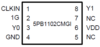
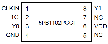
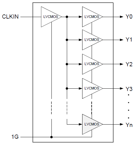
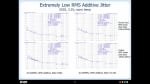
The 5PB1102 is a high-performance 1:2 LVCMOS clock buffer that offers a best-in-class additive phase jitter of 50fs RMS. This clock buffer also supports an Output Enable function. It is available in 8-pin DFN and TSSOP packages and can operate from a 1.8V to 3.3V supply.
特長
- High-performance 1:2 LVCMOS clock buffer
- Very low pin-to-pin skew: < 50ps
- Very low additive jitter: < 50fs
- Supply voltage: 1.8V to 3.3V
- fMAX = 200MHz
- Integrated serial termination for 50Ω channel
- Packaged in 8-pin TSSOP and small DFN packages
- Extended (-40 °C to +105 °C) temperature range
製品比較
アプリケーション
- Industrial applications
- Automotive
- Radar, LiDAR, and other applications
設計・開発
モデル
ECADモデル
[製品選択]テーブル内の製品名をクリックするとSamacSysが提供する回路図シンボル、PCBフットプリント、3D CADモデルがご確認いただけます。 お探しのシンボルやモデルが見つからない場合、Webサイトから直接リクエストできます。

製品選択
適用されたフィルター
ビデオ&トレーニング
5PB11xx Ultra Low Jitter LVCMOS Buffers
This video provides an overview of the LVCMOS High Performance Clock Buffer Family, highlighting their key features and capabilities.

Video List
ニュース&ブログ
| Buff Up Your Design with Renesas Clock Buffers | ブログ | 2018年12月15日 |
| IDT社が超低ジッターのLVCMOSクロックバッファ製品ファミリーを開発 | ニュース | 2015年3月30日 |