
High Speed A/D Converter Evaluation Kits
Renesas offers two options for evaluating high-speed analog-to-digital converter (ADC) products with LVDS and/or LVCMOS outputs. A complete, turnkey evaluation platform...
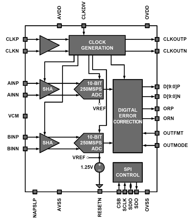
The KAD5610P is a family of low-power, high performance, dual-channel 10-bit, analog-to-digital converters. Designed with Intersil’s proprietary FemtoCharge™ technology on a standard CMOS process, the family supports sampling rates of up to 250MSPS. The KAD5610P-25 is the fastest member of this pin-compatible family, which also features sample rates of 210MSPS (KAD5610P-21), 170MSPS (KAD5610P-17) and 125MSPS (KAD5610P-12). A Serial Peripheral Interface (SPI) port allows for extensive configurability, as well as fine control of gain, skew and offset matching between the two converter cores. Digital output data is presented in selectable LVDS or CMOS formats. The KAD5610P is available in a 72 Ld QFN package with an exposed paddle. Performance is specified over the full industrial temperature range (-40°C to +85°C).
|
|
|
|
|---|---|---|
| 分類 | タイトル | 日時 |
| データシート | PDF 1.51 MB | |
| カタログ | PDF 5.67 MB English | |
| 製品変更通知 | PDF 322 KB | |
| ガイド | PDF 1.02 MB | |
| マニュアル-開発ツール | PDF 509 KB | |
| アプリケーションノート | PDF 296 KB | |
| アプリケーションノート | PDF 503 KB | |
| アプリケーションノート | PDF 1.08 MB | |
| アプリケーションノート | PDF 287 KB | |
9件
|
||
Renesas offers two options for evaluating high-speed analog-to-digital converter (ADC) products with LVDS and/or LVCMOS outputs. A complete, turnkey evaluation platform...
[製品選択]テーブル内の製品名をクリックするとSamacSysが提供する回路図シンボル、PCBフットプリント、3D CADモデルがご確認いただけます。 お探しのシンボルやモデルが見つからない場合、Webサイトから直接リクエストできます。

適用されたフィルター