概要
説明
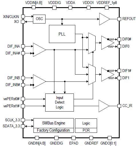
The 9FGL6241 is an intelligent buffer/clock generator tailored for single and dual-ported nVME SSDs. It supports Common (CC) and Independent Reference (IR) clocking architectures and is ideal for U.2 and M.2 form factors. The device is also useful in PCIe master/slave and clock multiplexing applications, with an internal clock generator as a third input channel.
For information regarding evaluation boards and material, please contact your local sales representative.
特長
- Automatically detects the presence or absence of input clocks and switches clock modes
- One open-drain CC_IR output indicates PCIe clock mode
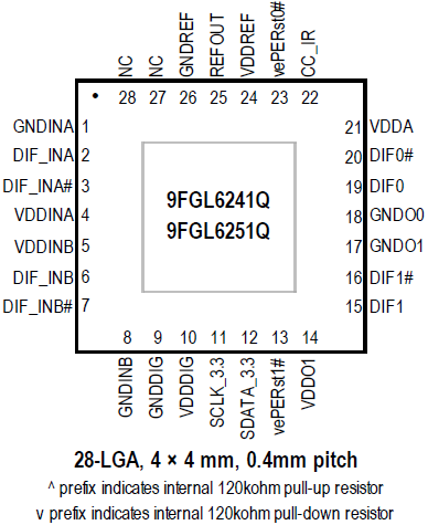
- Integrated crystal option available (Q option)
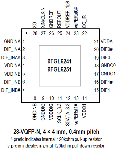
- Two 100MHz Low-power HCSL (LP-HCSL) outputs; 100Ω output impedance
- Integrated terminations on DIF outputs save 8 resistors
- 201, 301 configurations for SRnS (IR) or CC architectures default to 0% SSC
- 202, 302 configurations for SRIS (IR) or CC architectures default to -0.5% SSC
- SMBus-selectable -0.25% SSC
- Choice of 25MHz or 33 1/3MHz reference clock
- REF clock output saves external XO
- 2.5V or 3.3V operating voltage (VDDREF is 1.8V)
- 4mm × 4mm 28-VQFP-N package with external crystal
- 4mm × 4mm 28-LGA package with optional internal crystal
- Easy AC coupling to other logic families, see application note AN-891
- For devices with 85Ω output impedance, see 9FGL6251
製品比較
アプリケーション
設計・開発
ソフトウェア/ツール
モデル
ECADモデル
SamacSysの回路図シンボル、PCBフットプリント、および3D CADモデルは、製品オプションテーブルのCADモデルリンクをクリックすることで参照できます。シンボルまたはモデルが対応していない場合は、SamacSysに直接リクエスト可能です。

製品選択
適用されたフィルター
ビデオ&トレーニング
PCIe Reference Clock Jitter Budgets
Ron Wade, chief PCIe system architect explains the fundamental difference in reference clock jitter budgets between the first three generations of the specification and those of Gen4 and Gen5 which raise new challenges for designers.
Related Resources
Video List