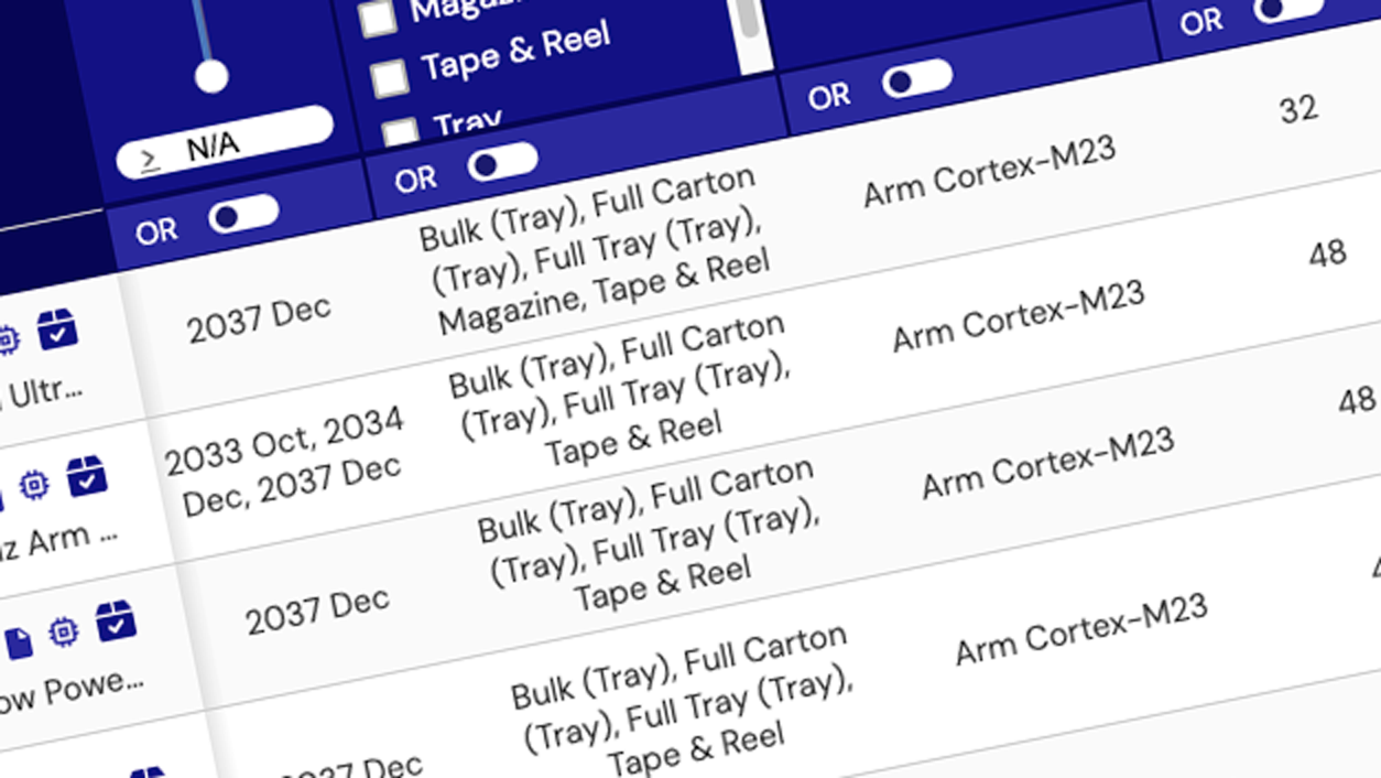
Renesas FemtoClock® NG Universal Frequency Translators™ (UFT™ ) cover all your frequency synthesis, frequency translation and jitter attenuation needs. Family members are available that support 1, 2, 3 or 4 PLLs in a single package.
As a frequency synthesizer, a low-cost, readily available fundamental mode crystal can be used to generate output frequencies that range from 1MHz to 1.3GHz. The internal architecture of the Universal Frequency Translator allows any frequency of crystal from 16 MHz to 40 MHz to be used regardless of the frequency desired.
As a frequency translator, this family of devices accepts 1 or 2 input reference clocks per PLL from 8kHz to 710MHz, switching between them as necessary, and generates any output frequency from 1MHz to 1.3GHz with no frequency translation error in most cases.
Members of the Universal Frequency Translator family support either one or two different pin-selectable configurations per PLL that may be pre-loaded into the internal one-time programmable (OTP) non-volatile memory for automatic operation directly from power up, or an I2C serial interface can be used to set the desired frequency translation configurations.
In addition to a crystal input, the Universal Frequency Translator (UFT) features two clock inputs per PLL and provides two outputs per PLL. Each output is individually programmable as LVPECL or LVDS. Versions of the Universal Frequency Translator with single-ended outputs are also available. Selection between the two input references per PLL may be performed manually via either pin or register, or it may be performed automatically with revertive or non-revertive recovery.
The devices can be used in the following modes of operation:
- Frequency Synthesizer Mode allows an arbitrary output frequency to be generated from a fundamental mode crystal input. The PLL feedback loop supports a fractional feedback divider. This allows the VCO operating frequency to be a non-integer multiple of the crystal frequency.
- High-Bandwidth Frequency Translator Mode is used to translate one or two input clocks of the same nominal frequency into an unrelated output frequency, attenuating cycle-to-cycle jitter. Only the High-Bandwidth PLL loop is used. A pre-divider stage is available, enabling input frequencies up to 710MHz.
- Low-Bandwidth Frequency Translator Mode (Jitter Attenuator Mode) involves two PLL loops and is typically used to achieve precise output-to-input frequency translation ratios. The Low-Bandwidth PLL loop drives a digitally controlled crystal oscillator (DCXO) loop via an analog-to-digital converter. The phase detector is optimized to work with frequencies starting at 8 kHz. An external low-pass filter can be used.
About Frequency Translators
A frequency translator is used to convert the frequency of the input signal to the frequency required for the output signal. These devices typically consist of an oscillator or PLL, and a frequency mixer. In some devices, a jitter attenuator circuit may be integrated with the frequency translator to simplify the circuit and minimize the bill-of-materials (BOM). Renesas’ rich portfolio of jitter attenuators and frequency translators can address the needs of virtually any application.