Overview
Description
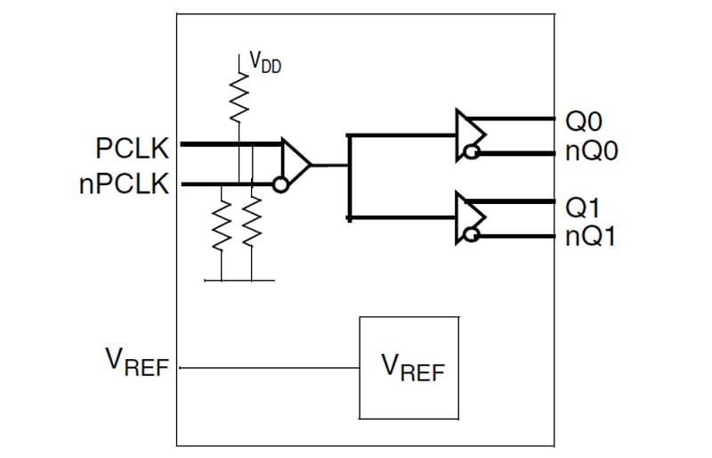
The 8P34S1102 is a high-performance differential LVDS fanout buffer. The device is designed for the fanout of 1PPS signals or high-frequency, very low additive phase noise clock and data signals. The 8P34S1102 supports fail-safe operation and is characterized to operate from a 1.8V or 2.5V power supply. Guaranteed output-to-output and part-to-part skew characteristics make the 8P34S1102 ideal for those clock distribution applications demanding well-defined performance and repeatability. One differential input and two low skew outputs are available. The integrated bias voltage reference enables easy interfacing of single-ended signals to the differential device input. The device is optimized for low power consumption and low additive phase noise.
Features
- Two low skew, low additive jitter LVDS output pairs
- One differential clock input pair
- Differential CLK, nCLK pairs can accept the following differential input levels: LVDS, CML
- Maximum input clock frequency: 1.2GHz
- Output skew: 3ps (typical)
- Propagation delay: 400ps (maximum)
- Low additive phase jitter, RMS; fREF = 156.25MHz, 10kHz to 20MHz: 34fs (typical)
- Device current consumption (IDD):
- 40mA typical: 1.8V
- 50mA typical: 2.5V
- Full 1.8V or 2.5V supply voltage
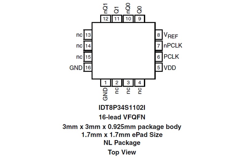
- Lead-free (RoHS 6), 16-lead VFQFN package
- -40 °C to 85 °C ambient operating temperature
- Supports case temperature up to +105 °C
- Supports PCI Express Gen 1-5
Comparison
Applications
Design & Development
Models
ECAD Models
Schematic symbols, PCB footprints, and 3D CAD models from SamacSys can be found by clicking on the CAD Model links in the Product Options table. If a symbol or model isn't available, it can be requested directly from SamacSys.

Product Options
Applied Filters: