Overview
Description
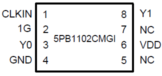
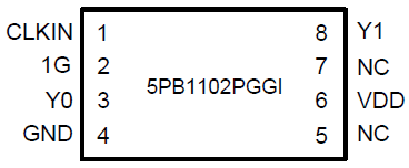
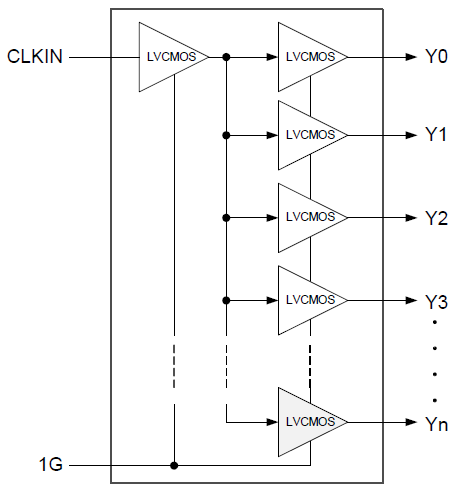
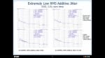
The 5PB1102 is a high-performance 1:2 LVCMOS clock buffer that offers a best-in-class additive phase jitter of 50fs RMS. This clock buffer also supports an Output Enable function. It is available in 8-pin DFN and TSSOP packages and can operate from a 1.8V to 3.3V supply.
Features
- High-performance 1:2 LVCMOS clock buffer
- Very low pin-to-pin skew: < 50ps
- Very low additive jitter: < 50fs
- Supply voltage: 1.8V to 3.3V
- fMAX = 200MHz
- Integrated serial termination for 50Ω channel
- Packaged in 8-pin TSSOP and small DFN packages
- Extended (-40 °C to +105 °C) temperature range
Comparison
Applications
- Industrial applications
- Automotive
- Radar, LiDAR, and other applications
Design & Development
Models
ECAD Models
Schematic symbols, PCB footprints, and 3D CAD models from SamacSys can be found by clicking on the CAD Model links in the Product Options table. If a symbol or model isn't available, it can be requested directly from SamacSys.

Product Options
Applied Filters:
Videos & Training
5PB11xx Ultra Low Jitter LVCMOS Buffers
This video provides an overview of the LVCMOS High Performance Clock Buffer Family, highlighting their key features and capabilities.
Related Resources

Video List
News & Blog Posts
| Buff Up Your Design with Renesas Clock Buffers | Blog Post | Dec 15, 2018 |
| IDT Introduces Ultra-Low-Jitter Family of LVCMOS Clock Buffers | News | Mar 24, 2015 |