Overview
Description
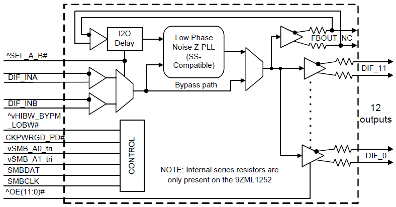
The 9ZML1232E is a second-generation 2-input/12-output differential mux for Intel Purley and newer platforms. It exceeds the demanding DB1200ZL performance specifications and is backward compatible with the 9ZML1232B. The device utilizes Low Power HCSL-compatible outputs to reduce power consumption and termination resistors. It is suitable for PCI Express Gen 1-4 or QPI/UPI applications, and provides two configurable low-drift I2O settings, one for each input channel, to allow I2O tuning for various topologies.

Features
- 2 configurable low-drift I2O delays up to 2.9ns; maintain transport delay for various topologies
- LP-HCSL outputs; eliminate 24 resistors
- 9 selectable SMBus addresses; multiple devices can share the same SMBus segment
- Separate VDDIO for outputs; allows maximum power savings
- PLL or Bypass Mode; PLL can de-jitter incoming clock
- Hardware or software-selectable PLL BW; minimizes jitter peaking in downstream PLLs
- Spread spectrum compatible; tracks spreading input clock for EMI reduction
- SMBus interface; software can modify device settings without hardware changes
- 10mm x 10mm 72-QFN package; small board footprint
Comparison
Applications
Design & Development
Boards & Kits
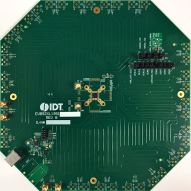
Evaluation
EVK9ZXL1951D
Active
Evaluation Kit for 19-Output DB1900Z for PCIe Gen1-4 and QPI/UPI
The evaluation board is designed to help the customer evaluate the 9ZXL1951D. The device is programmable through an SMBus interface. The user guide details the board set and connection, as well as the companion Graphical User Interface (GUI) installation for communicating with the device. The...
Recommended Documents:
Models
ECAD Models
Schematic symbols, PCB footprints, and 3D CAD models from SamacSys can be found by clicking on the CAD Model links in the Product Options table. If a symbol or model isn't available, it can be requested directly from SamacSys.

Product Options
Applied Filters:
Videos & Training
PCIe Gen5 Clock Buffers
Introducing Renesas’ enhanced PCIe clock buffer family. These PCIe Gen5 clock buffers offer fanout and zero-delay operating modes, supporting both legacy systems and the most complex timing trees within a single device. Unlike many existing solutions, whose performance limitations force their use in fanout buffer mode, these clock buffers meet both PCIe Gen5 and prominent CPU-specific phase jitter requirements in all operating modes. The extremely low 50fs rms PCIe Gen5 additive phase jitter enables multi-level cascading within the strict PCIe Gen5 jitter budget. Renesas’ high-performance oscillators and clock generators provide an ideal clock source for the enhanced PCIe clock buffer family.
For more information about these PCIe Gen5 clock buffers, visit the PCIe timing page.
Video List