Automatic Liquid Dispenser Reference Design
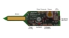
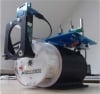
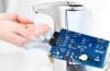
This Automatic Liquid Dispenser reference design is for hands-free dispensing of liquids such as soap, hand sanitizer, shampoos, or hand lotions. Automatic liquid...

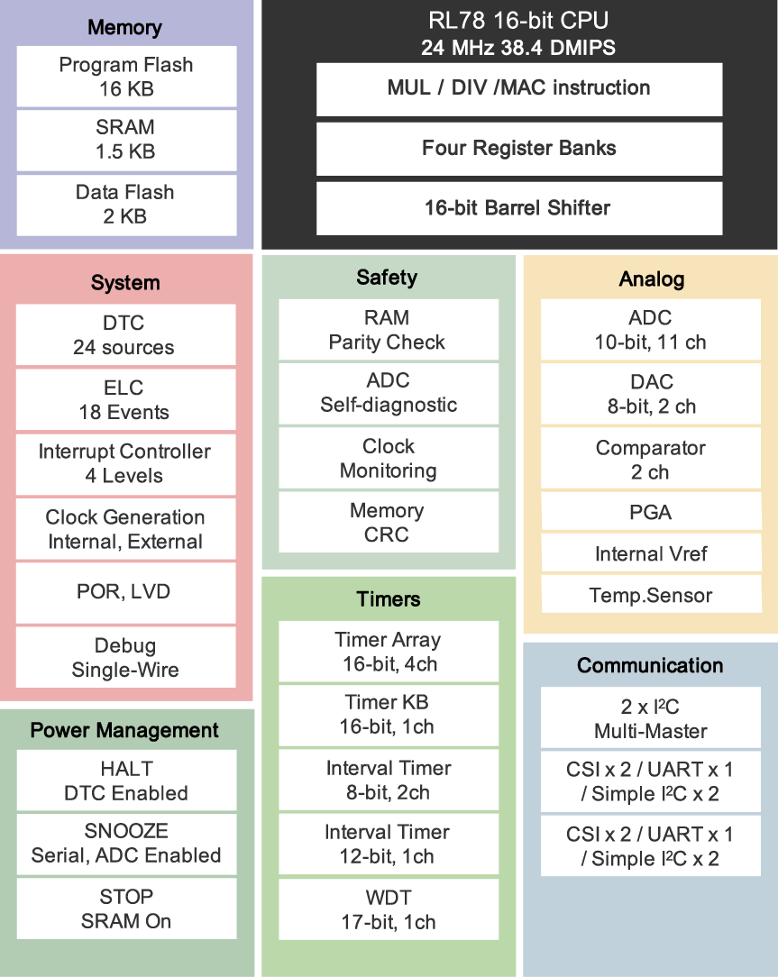
The RL78/G11 microcontroller line-up concept is based on small packages like 10 to 25pin, in small 16KB flash memory and rich analog peripherals such as A/D converters, D/A converters, comparators and PGA and these are configurable as PGA+ADC+VBGR, PGA+CMP, CMP+DAC/VBGR, or PGA+CMP+DAC/VBGR. Using the smart features like DTC and ELC a lot of peripherals can be connected internally to reduce CPU workload and can save overall power consumption. It also supports very low power operation (100 uA @ 1 MHz ) and a high speed 4µs wake up. Available in small 3x3mm² WFLGA , 3x3mm² HWQFN and standard 20pin LSSOP, this MCU line is suitable for sensor application, Lighting/power sources and many small appliances.
| Software title
|
Software type
|
Company
|
|---|---|---|
| Sound Playback/Compression System [M3S-S2-Tiny] for RL78 Family Sound playback system for RL78 Family
|
Sound / Voice | Renesas |
| AP4, Applilet Peripheral I/O driver generator compatible with third-party compilers and GNU compiler (for RZ, V850, RX, RL78, and 78K)
|
Code Generator | Renesas |
| Applilet EZ PL for RL78 Programming software that can easily create microcontroller application software like assembling a puzzle, without using programming languages
|
Code Generator | Renesas |
| Code Generator Plug-in Automatic driver generation tool for internal peripheral I/O modules through GUI settings [Standard features for Renesas IDE "e² studio" and CS+] [Support MCU/MPU: RL78, V850, 78K, RX]
|
Code Generator | Renesas |
| C Compiler Package for RL78 Family [CC-RL] C Compiler Package for RL78 Family [IDE: CS+, e² studio]
|
Compiler/Assembler | Renesas |
| E2 emulator [RTE0T00020KCE00000R] On-chip debugging emulator. Also available as a flash memory programmer. [Support MCU/MPU: RA, RE, RH850, R-Car D1, RL78, RX, RISC-V MCU]
|
Emulator | Renesas |
| E2 emulator Lite [RTE0T0002LKCE00000R] On-chip debugging emulator. Also available as a flash memory programmer. [Support MCU/MPU: RA, RE, RL78, RX, RISC-V MCU]
|
Emulator | Renesas |
| PG-FP6 Flash memory programmer [Programming software: Dedicated GUI-based software, the "FP6 Terminal"] [Support MCU/MPU and devices: RA, RE, RX, RL78, RH850, RISC-V MCU, Renesas Synergy, Power Management, Renesas USB Power Delivery Family, ICs for Motor Driver/Actuator Driver, SuperH RISC engine, V850, 78K, R8C]
|
Programmer (Unit/SW) | Renesas |
| Renesas Flash Programmer (Programming GUI) Flash memory programming software [Support MCU/MPU and devices: RA, RE, RX, RL78, RH850, RISC-V MCU Renesas Synergy, DA1459x, DA1469x, DA1470x, Power Management, Renesas USB Power Delivery Family, ICs for Motor Driver/Actuator Driver, V850, 78K0R, 78K0]
|
Programmer (Unit/SW) | Renesas |
| Code Flash Libraries (Flash Self Programming Libraries) Libraries for the reprogramming of code area flash memory, including EEPROM emulation libraries for the code areas of 78K-family products
|
Self Programming Library (Flash Library) | Renesas |
| Data Flash Libraries Libraries for the reprogramming of data flash memory, including EEPROM emulation libraries for the data areas of RL78-family products
|
Self Programming Library (Flash Library) | Renesas |
| Simulator for e² studio of RL78 Family Simulator for RL78 Family [Support IDE: e² studio] (Note: This product is included in the Renesas IDE "e² studio" and is not available separately.)
|
Simulator | Renesas |
| RL78 Web Simulator Right online tools to support initial evaluation of the low power consumption RL78 Family. Lineup: MCU Simulator Online and Current Consumption Calculator. Free of charge.
|
Simulator | Renesas |
| QE for Current Consumption: A Dedicated Tool for Current Measurement Development assistance tool helps to shorten the times taken in operations for the tuning of currents drawn. [Standard item in the "e² studio" and CS+ (CS+ for CC only) IDEs] [Support MCU/MPU: RX, RL78]
|
Solution Toolkit | Renesas |
| CS+ Renesas integrated development environment (IDE) [Support MCU/MPU: RH850, V850, RX, RL78, 78K0R, 78K0]
(Note: CS+ is not generally promoted to U.S. and European customers.)
(Note: To use Smart Configurator on CS+ for RL78/G23 and RX family MCUs, install the Smart Configurator for each MCU family separately downloading from ”Design & Support” > ”Development Tools” > ”Smart Configurator”)
|
IDE and Coding Tool | Renesas |
| Sensor Software Modules for Renesas MCU Platforms Middleware (FIT module and FSP module) and sample software packages that enable control and data acquisition for Renesas sensor products.
|
Sensor | Renesas |
| e² studio - information for RL78 Family Eclipse-based Renesas integrated development environment (IDE).
|
IDE and Coding Tool | Renesas |
| Crypto Library Robust encode library to ensure security for all types of system developments
|
Security / Crypto | Renesas |
| SPI/QSPI Serial Flash Memory, QSPI Serial Phase Change Memory Driver Device Driver for SPI and QSPI Serial Flash Memory and QSPI Serial Phase Change Memory
|
Serial Memory | Renesas |
| IAR Embedded Workbench for Renesas RL78 IAR Embedded Workbench provides extensive support for RL78 devices. IAR Embedded Workbench is a complete set of development tools with leading optimization technology for creating powerful automotive applications.
|
IDE and Coding Tool | IAR Systems |
| Renesas IAR Embedded Workbench Device-Support-Packages Renesas IAR Embedded Workbench Device-Support-Packages include all device-specific files to be used with the Embedded Workbench IDE.
|
IDE and Coding Tool | Renesas |
|
21 items
|
||
This Automatic Liquid Dispenser reference design is for hands-free dispensing of liquids such as soap, hand sanitizer, shampoos, or hand lotions. Automatic liquid...
A popular appliance in many households, the gas stove requires a high demand for control and safety. This High-End Gas Cooker solution enables real-time gas...
Temperature, humidity and luminance changes in the air have a direct impact on human body comfort and emotions; as a result, the detection of these factors is very...
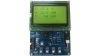
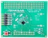
RPB (Renesas Promotion Board) with RL78/G11 MCU is a small board ideal for prototyping/evaluation. We packed the E2 emulator Lite debugger/programmer function, the...
The Safety Light Curtain is an optoelectronic device that is used to safeguard personnel in the vicinity of moving machinery with the potential to cause harm such as...
Human health, in both developing and developed countries throughout the world, depends on the quality of available drinking water. As a result, water quality testing is...
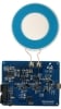
Wireless charging is a technology that uses the principle of electromagnetic induction to transfer electrical energy between two coils. It has been installed as one of...
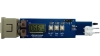
The Wireless Doorbell application uses sub-GHz wireless communication to notify a remote receiver when the doorbell is pressed. The transmitter and receiver both have a...
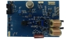
The YQB-R5F1057A-TB is a target board used for evaluating RL78/G11 microcontroller operations using a Renesas E1 or E2 Lite on-chip debugging emulator/flash programmer.
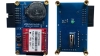
The Smart Moisture Sensor solution uses the RL78/G11 MCU's moisture sensor to measure the conditions of soil, and transfer the data to a smartphone app via an RL78/G1D...
This design easily attaches the sensor board to any type of mechanical water meter with metalized index wheel and detects with it, both RPM as well as the rotation...
Schematic symbols, PCB footprints, and 3D CAD models from SamacSys can be found by clicking on products in the Product Options table. If a symbol or model isn't available, it can be requested directly from the website.

PLP |
Program Memory (KB) |
RAM (KB) |
Lead Count (#) |
Temp. Range |
Bit Size |
CPU |
Data Flash (KB) |
Supply Voltage (V) |
Operating Freq (Max) (MHz) |
RTC |
LVD |
DMA |
I/O Ports |
Timer |
ADC |
DAC |
CAN (ch) |
Ethernet |
USB |
Human Machine Interface |
Moisture Sensitivity Level (MSL) |
Price (USD) | 1ku |
Buy / Sample |
|
|---|---|---|---|---|---|---|---|---|---|---|---|---|---|---|---|---|---|---|---|---|---|---|---|---|
| Part Number | ||||||||||||||||||||||||
| 2035 Dec | 16 | 1.5 | 20 | -40 to 85°C | 16 | RL78 | 2 | 1.6 - 5.5 | 24 | Yes | Yes | No | 17 | 8-bit x 2-ch, 12-bit x 1-ch, 16-bit x 5-ch | 10-bit x 10-ch | 8-bit x 2-ch | 0 | No | 3 | 1.661 | Get Samples, | |||
| 2035 Dec | 16 | 1.5 | 20 | -40 to 85°C | 16 | RL78 | 2 | 1.6 - 5.5 | 24 | Yes | Yes | No | 17 | 8-bit x 2-ch, 12-bit x 1-ch, 16-bit x 5-ch | 10-bit x 10-ch | 8-bit x 2-ch | 0 | No | 3 | |||||
| 2035 Dec | 16 | 1.5 | 20 | -40 to 105°C | 16 | RL78 | 2 | 1.6 - 5.5 | 24 | Yes | Yes | No | 17 | 8-bit x 2-ch, 12-bit x 1-ch, 16-bit x 5-ch | 10-bit x 10-ch | 8-bit x 2-ch | 0 | No | 3 | 1.184 | Get Samples, | |||
| 2035 Dec | 16 | 1.5 | 20 | -40 to 105°C | 16 | RL78 | 2 | 1.6 - 5.5 | 24 | Yes | Yes | No | 17 | 8-bit x 2-ch, 12-bit x 1-ch, 16-bit x 5-ch | 10-bit x 10-ch | 8-bit x 2-ch | 0 | No | 3 | |||||
| N/A | 16 | 1.5 | 10 | -40 to 105°C | 16 | RL78 | 2 | 1.6 - 5.5 | 24 | Yes | Yes | No | 7 | 8-bit x 2-ch, 12-bit x 1-ch, 16-bit x 5-ch | 10-bit x 3-ch | 8-bit x 1-ch | 0 | No | 3 | Get Samples, | ||||
| 2035 Dec | 16 | 1.5 | 10 | -40 to 105°C | 16 | RL78 | 2 | 1.6 - 5.5 | 24 | Yes | Yes | No | 7 | 8-bit x 2-ch, 12-bit x 1-ch, 16-bit x 5-ch | 10-bit x 3-ch | 8-bit x 1-ch | 0 | No | 3 | |||||
| N/A | 16 | 1.5 | 10 | -40 to 85°C | 16 | RL78 | 2 | 1.6 - 5.5 | 24 | Yes | Yes | No | 7 | 8-bit x 2-ch, 12-bit x 1-ch, 16-bit x 5-ch | 10-bit x 3-ch | 8-bit x 1-ch | 0 | No | 3 | 0.6818 | Get Samples, | |||
| 2035 Dec | 16 | 1.5 | 10 | -40 to 85°C | 16 | RL78 | 2 | 1.6 - 5.5 | 24 | Yes | Yes | No | 7 | 8-bit x 2-ch, 12-bit x 1-ch, 16-bit x 5-ch | 10-bit x 3-ch | 8-bit x 1-ch | 0 | No | 3 | 0.6817 | ||||
| N/A | 16 | 1.5 | 25 | -40 to 85°C | 16 | RL78 | 2 | 1.6 - 5.5 | 24 | Yes | Yes | No | 21 | 8-bit x 2-ch, 12-bit x 1-ch, 16-bit x 5-ch | 10-bit x 11-ch | 8-bit x 2-ch | 0 | No | 3 | |||||
| N/A | 16 | 1.5 | 25 | -40 to 85°C | 16 | RL78 | 2 | 1.6 - 5.5 | 24 | Yes | Yes | No | 21 | 8-bit x 2-ch, 12-bit x 1-ch, 16-bit x 5-ch | 10-bit x 11-ch | 8-bit x 2-ch | 0 | No | 3 | |||||
| N/A | 16 | 1.5 | 25 | -40 to 105°C | 16 | RL78 | 2 | 1.6 - 5.5 | 24 | Yes | Yes | No | 21 | 8-bit x 2-ch, 12-bit x 1-ch, 16-bit x 5-ch | 10-bit x 11-ch | 8-bit x 2-ch | 0 | No | 3 | |||||
| N/A | 16 | 1.5 | 25 | -40 to 105°C | 16 | RL78 | 2 | 1.6 - 5.5 | 24 | Yes | Yes | No | 21 | 8-bit x 2-ch, 12-bit x 1-ch, 16-bit x 5-ch | 10-bit x 11-ch | 8-bit x 2-ch | 0 | No | 3 | |||||
| N/A | 16 | 1.5 | 16 | -40 to 85°C | 16 | RL78 | 2 | 1.6 - 5.5 | 24 | Yes | Yes | No | 13 | 8-bit x 2-ch, 12-bit x 1-ch, 16-bit x 5-ch | 10-bit x 8-ch | 8-bit x 2-ch | 0 | No | 3 | 0.7423 | Get Samples, | |||
| 2035 Dec | 16 | 1.5 | 16 | -40 to 85°C | 16 | RL78 | 2 | 1.6 - 5.5 | 24 | Yes | Yes | No | 13 | 8-bit x 2-ch, 12-bit x 1-ch, 16-bit x 5-ch | 10-bit x 8-ch | 8-bit x 2-ch | 0 | No | 3 | 0.7423 | ||||
| N/A | 16 | 1.5 | 16 | -40 to 105°C | 16 | RL78 | 2 | 1.6 - 5.5 | 24 | Yes | Yes | No | 13 | 8-bit x 2-ch, 12-bit x 1-ch, 16-bit x 5-ch | 10-bit x 8-ch | 8-bit x 2-ch | 0 | No | 3 | 0.9373 | Get Samples, | |||
| 2035 Dec | 16 | 1.5 | 16 | -40 to 105°C | 16 | RL78 | 2 | 1.6 - 5.5 | 24 | Yes | Yes | No | 13 | 8-bit x 2-ch, 12-bit x 1-ch, 16-bit x 5-ch | 10-bit x 8-ch | 8-bit x 2-ch | 0 | No | 3 | |||||
| 2035 Dec | 16 | 1.5 | 24 | -40 to 85°C | 16 | RL78 | 2 | 1.6 - 5.5 | 24 | Yes | Yes | No | 21 | 8-bit x 2-ch, 12-bit x 1-ch, 16-bit x 5-ch | 10-bit x 11-ch | 8-bit x 2-ch | 0 | No | 3 | |||||
| N/A | 16 | 1.5 | 24 | -40 to 105°C | 16 | RL78 | 2 | 1.6 - 5.5 | 24 | Yes | Yes | No | 21 | 8-bit x 2-ch, 12-bit x 1-ch, 16-bit x 5-ch | 10-bit x 11-ch | 8-bit x 2-ch | 0 | No | 3 | |||||
| 2035 Dec | 16 | 1.5 | 24 | -40 to 105°C | 16 | RL78 | 2 | 1.6 - 5.5 | 24 | Yes | Yes | No | 21 | 8-bit x 2-ch, 12-bit x 1-ch, 16-bit x 5-ch | 10-bit x 11-ch | 8-bit x 2-ch | 0 | No | 3 | |||||
| N/A | 16 | 1.5 | 24 | -40 to 85°C | 16 | RL78 | 2 | 1.6 - 5.5 | 24 | Yes | Yes | No | 21 | 8-bit x 2-ch, 12-bit x 1-ch, 16-bit x 5-ch | 10-bit x 11-ch | 8-bit x 2-ch | 0 | No | 3 | |||||
| N/A | 16 | 1.5 | 20 | -40 to 85°C | 16 | RL78 | 2 | 1.6 - 5.5 | 24 | Yes | Yes | No | 17 | 8-bit x 2-ch, 12-bit x 1-ch, 16-bit x 5-ch | 10-bit x 10-ch | 8-bit x 2-ch | 0 | No | 3 | 1.081 | ||||
| 2035 Dec | 16 | 1.5 | 20 | -40 to 85°C | 16 | RL78 | 2 | 1.6 - 5.5 | 24 | Yes | Yes | No | 17 | 8-bit x 2-ch, 12-bit x 1-ch, 16-bit x 5-ch | 10-bit x 10-ch | 8-bit x 2-ch | 0 | No | 3 | |||||
| N/A | 16 | 1.5 | 20 | -40 to 105°C | 16 | RL78 | 2 | 1.6 - 5.5 | 24 | Yes | Yes | No | 17 | 8-bit x 2-ch, 12-bit x 1-ch, 16-bit x 5-ch | 10-bit x 10-ch | 8-bit x 2-ch | 0 | No | 3 | 1.132 | ||||
| 2035 Dec | 16 | 1.5 | 20 | -40 to 105°C | 16 | RL78 | 2 | 1.6 - 5.5 | 24 | Yes | Yes | No | 17 | 8-bit x 2-ch, 12-bit x 1-ch, 16-bit x 5-ch | 10-bit x 10-ch | 8-bit x 2-ch | 0 | No | 3 | |||||
| 2035 Dec | 16 | 1.5 | 16 | -40 to 85°C | 16 | RL78 | 2 | 1.6 - 5.5 | 24 | Yes | Yes | No | 13 | 8-bit x 2-ch, 12-bit x 1-ch, 16-bit x 5-ch | 10-bit x 8-ch | 8-bit x 2-ch | 0 | No | 3 | |||||
| N/A | 16 | 1.5 | 16 | -40 to 85°C | 16 | RL78 | 2 | 1.6 - 5.5 | 24 | Yes | Yes | No | 13 | 8-bit x 2-ch, 12-bit x 1-ch, 16-bit x 5-ch | 10-bit x 8-ch | 8-bit x 2-ch | 0 | No | 3 | 0.8278 | ||||
| 2035 Dec | 16 | 1.5 | 16 | -40 to 85°C | 16 | RL78 | 2 | 1.6 - 5.5 | 24 | Yes | Yes | No | 13 | 8-bit x 2-ch, 12-bit x 1-ch, 16-bit x 5-ch | 10-bit x 8-ch | 8-bit x 2-ch | 0 | No | 3 | 0.8278 | ||||
| 2035 Dec | 16 | 1.5 | 16 | -40 to 105°C | 16 | RL78 | 2 | 1.6 - 5.5 | 24 | Yes | Yes | No | 13 | 8-bit x 2-ch, 12-bit x 1-ch, 16-bit x 5-ch | 10-bit x 8-ch | 8-bit x 2-ch | 0 | No | 3 | |||||
| N/A | 16 | 1.5 | 16 | -40 to 105°C | 16 | RL78 | 2 | 1.6 - 5.5 | 24 | Yes | Yes | No | 13 | 8-bit x 2-ch, 12-bit x 1-ch, 16-bit x 5-ch | 10-bit x 8-ch | 8-bit x 2-ch | 0 | No | 3 | 1.081 | ||||
| 2035 Dec | 16 | 1.5 | 16 | -40 to 105°C | 16 | RL78 | 2 | 1.6 - 5.5 | 24 | Yes | Yes | No | 13 | 8-bit x 2-ch, 12-bit x 1-ch, 16-bit x 5-ch | 10-bit x 8-ch | 8-bit x 2-ch | 0 | No | 3 | |||||
| 2035 Dec | 16 | 1.5 | 24 | -40 to 85°C | 16 | RL78 | 2 | 1.6 - 5.5 | 24 | Yes | Yes | No | 21 | 8-bit x 2-ch, 12-bit x 1-ch, 16-bit x 5-ch | 10-bit x 11-ch | 8-bit x 2-ch | 0 | No | 3 | |||||
| 2035 Dec | 16 | 1.5 | 24 | -40 to 105°C | 16 | RL78 | 2 | 1.6 - 5.5 | 24 | Yes | Yes | No | 21 | 8-bit x 2-ch, 12-bit x 1-ch, 16-bit x 5-ch | 10-bit x 11-ch | 8-bit x 2-ch | 0 | No | 3 | |||||
| 2035 Dec | 16 | 1.5 | 10 | -40 to 85°C | 16 | RL78 | 2 | 1.6 - 5.5 | 24 | Yes | Yes | No | 7 | 8-bit x 2-ch, 12-bit x 1-ch, 16-bit x 5-ch | 10-bit x 3-ch | 8-bit x 1-ch | 0 | No | 3 | |||||
| 2035 Dec | 16 | 1.5 | 10 | -40 to 105°C | 16 | RL78 | 2 | 1.6 - 5.5 | 24 | Yes | Yes | No | 7 | 8-bit x 2-ch, 12-bit x 1-ch, 16-bit x 5-ch | 10-bit x 3-ch | 8-bit x 1-ch | 0 | No | 3 | |||||
| 2035 Dec | 16 | 1.5 | 16 | -40 to 85°C | 16 | RL78 | 2 | 1.6 - 5.5 | 24 | Yes | Yes | No | 13 | 8-bit x 2-ch, 12-bit x 1-ch, 16-bit x 5-ch | 10-bit x 8-ch | 8-bit x 2-ch | 0 | No | 3 | |||||
| 2035 Dec | 16 | 1.5 | 16 | -40 to 105°C | 16 | RL78 | 2 | 1.6 - 5.5 | 24 | Yes | Yes | No | 13 | 8-bit x 2-ch, 12-bit x 1-ch, 16-bit x 5-ch | 10-bit x 8-ch | 8-bit x 2-ch | 0 | No | 3 | |||||
| 2035 Dec | 16 | 1.5 | 20 | -40 to 85°C | 16 | RL78 | 2 | 1.6 - 5.5 | 24 | Yes | Yes | No | 17 | 8-bit x 2-ch, 12-bit x 1-ch, 16-bit x 5-ch | 10-bit x 10-ch | 8-bit x 2-ch | 0 | No | 3 | |||||
| 2035 Dec | 16 | 1.5 | 20 | -40 to 105°C | 16 | RL78 | 2 | 1.6 - 5.5 | 24 | Yes | Yes | No | 17 | 8-bit x 2-ch, 12-bit x 1-ch, 16-bit x 5-ch | 10-bit x 10-ch | 8-bit x 2-ch | 0 | No | 3 |