概要
説明
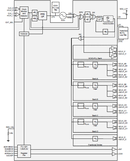
The 8V19N474 is a fully integrated FemtoClock® NG Jitter Attenuator and Clock Synthesizer designed as a high-performance clock solution for conditioning and frequency/phase management of 10/40/100/400 Gigabit-Ethernet line cards. The device is optimized to deliver excellent phase noise performance as required to drive physical layer devices and provides the clean clock frequencies of e.g. 625, 500, 312.5, 250, 156.25 and 125MHz. A two-stage PLL architecture supports both jitter attenuation and frequency multiplication. The first stage PLL is the jitter attenuator and uses an external VCXO for best possible phase noise characteristics. The second stage PLL locks on the VCXO-PLL output signal and synthesizes the target frequency. This PLL has a VCO circuit at 2500MHz.
The device generates the output clock signals from the VCO by frequency division. Five independent frequency dividers are available, four support integer-divider ratios and one integer as well as fractional-divider ratios. Delay circuits can be used for achieving alignment and controlled phase delay between clock signals. The two redundant inputs are monitored for activity. Four selectable clock switching modes are provided to handle clock input failure scenarios. Auto-lock, individually programmable output frequency dividers and phase adjustment capabilities are added for flexibility. The device is configured through an SPI interface and reports lock and signal loss status in internal registers and via an lock detect (LOCK) output. Internal status bit changes can also be reported via the nINT output. The device is ideal for driving converter circuits in wireless infrastructure, radar/imaging and instrumentation/medical applications.
For information regarding evaluation boards and material, please contact your local sales representative.
特長
- High-performance clock RF-PLL
- Optimized for low phase noise: -153dBc/Hz (1MHz offset; 156.25MHz clock)
- Integrated phase noise (12kHz-20MHz) of 75fs RMS typ.
- Dual-PLL architecture
- 1st-PLL stage with external VCXO for clock jitter attenuation
- 2nd-PLL stage with internal FemtoClock NG PLL at 2500MHz
- 6 output banks with a total of 12 outputs, organized in:
- Two clock banks with one integer frequency divider and three differential outputs
- Two clock banks with one integer frequency divider and two differential outputs
- One clock bank with one fractional output divider and one differential output
- One VCXO-PLL output bank with one selectable LVDS/two LVCMOS outputs
- Four output banks contain a phase delay circuit with steps of the VCO clock period (400ps)
- Supported clock output frequencies include:
- from the integer dividers: 2500, 1250, 625, 500, 312.5, 250, 156.25 and 125MHz
- from the fractional divider: 80 – 300MHz
- Low-power LVPECL/LVDS outputs support configurable signal amplitude, DC and AC coupling and LVPECL, LVDS line terminations techniques
- Redundant input clock architecture
- Two inputs
- Individual input signal monitor
- Digital holdover
- Manual and automatic clock selection
- Hitless switching
- Status monitoring and fault reporting
- Input signal status
- Hold-over and reference loss status
製品比較
アプリケーション
設計・開発
モデル
ECADモデル
[製品選択]テーブル内の製品名をクリックするとSamacSysが提供する回路図シンボル、PCBフットプリント、3D CADモデルがご確認いただけます。 お探しのシンボルやモデルが見つからない場合、Webサイトから直接リクエストできます。

| CABGA | 81 | I | Yes | Tray | 3 | 23.07 | サンプルを入手, | |
| CABGA | 81 | I | Yes | Reel | 3 |

Tips for Using This Parametric Table:
- Hide Filters button in header: Collapse or expands filters
- Column sort buttons in header: Sort Column alphabetically / numerically descending or ascending
- Reset button in header: Reset all filters to the page default
- Full Screen button in header: Expand the table to full screen view (user must close out of full screen before they can interact with rest of page)
- Export button in header: Export the filtered results of the table to an Excel document
- Filter parts search bar in header: Type to filter table results by part number
- Hide column button in column headers: Select to hide columns in table
- AND / OR toggle switches in header: Toggles the logic of this particular filter to be “AND” or “OR” logic for filtering results
- Multiselect checkboxes at beginning of each row in table: Select these checkboxes to compare products against each other
- Document icon next to product name in row: View the featured document for this product
- Chip icon next to the right of the document icon in row: View the block diagram for this product
- Cart icon to the right of the chip icon: Indicates that samples are available for this product
ビデオ&トレーニング
ニュース&ブログ
| ブログ | 2021年4月27日 | ||
| IDT、100Gと400Gアプリケーション向けに、 業界をリードする位相ノイズ性能の最新タイミング製品を発表 | ニュース | 2017年12月20日 |
