概要
説明
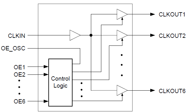
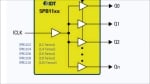
The 5PB1213 is a high-performance TCXO/LVCMOS clock fanout buffer with individual OE pins for each output. The CLKIN pin can accept either a square wave (LVCMOS) or a clipped sine wave (such as TCXO clipped sine wave output) as input.
The 5PB1213 has industry-leading low jitter and extremely low current consumption, making it ideal for smart mobile devices.

特長
- Extremely low operating and standby current consumption
- Low RMS Additive Phase jitter
- 2.5V to 3.3V power supply voltage
- Three outputs with individual Output Enable pin
- One input
- OE_OSC control pin to enable/disable reference TCXO/XO
- Small 10-pin DFN package
- Extended temperature range (-40 °C to +105 °C)
製品比較
アプリケーション
- Smart mobile handsets
- RF and baseband peripheral clock distribution
- Automotive
ドキュメント
ピックアップ
ログイン後、ご登録が可能となります。
|
|
|
|
|---|---|---|
| 分類 | タイトル | 日時 |
| データシート | PDF 292 KB | |
| アプリケーションノート | PDF 187 KB | |
| 概要 | PDF 217 KB | |
| 製品変更通知 | PDF 129 KB | |
| 概要 | PDF 252 KB | |
| アプリケーションノート | PDF 495 KB | |
| アプリケーションノート | PDF 442 KB | |
| アプリケーションノート | PDF 565 KB | |
8件
|
||
設計・開発
モデル
ECADモデル
[製品選択]テーブル内の製品名をクリックするとSamacSysが提供する回路図シンボル、PCBフットプリント、3D CADモデルがご確認いただけます。 お探しのシンボルやモデルが見つからない場合、Webサイトから直接リクエストできます。

製品選択
適用されたフィルター
ビデオ&トレーニング
5PB11xx Ultra Low Jitter LVCMOS Buffers
This video provides an overview of the LVCMOS High Performance Clock Buffer Family, highlighting their key features and capabilities.
Related Resources

Video List
ニュース&ブログ
| IDT社が超低ジッターのLVCMOSクロックバッファ製品ファミリーを開発 | ニュース | 2015年3月30日 |