概要
説明
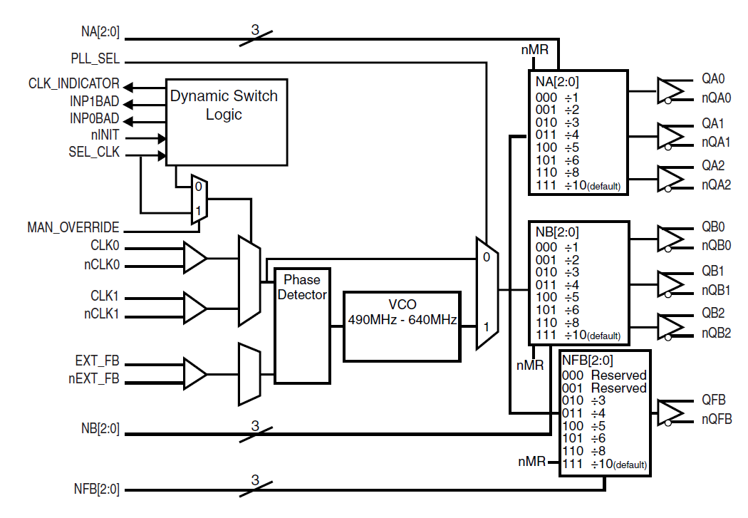
The 873995 is a Zero Delay/Multiplier/Divider with hitless input clock switching capability. The 873995 is ideal for use in redundant, fault tolerant clock trees where low phase noise and low jitter are critical. The device receives two differential LVPECL clock signals from which it generates 6 LVPECL clock outputs with "zero" delay. The output divider and feedback divider selections also allow for frequency multiplication or division. The 873995 Dynamic Clock Switch (DCS) circuit continuously monitors both input clock signals. Upon detection of a failure (input clock stuck LOW or HIGH for at least 1 period), INP_BAD for that clock will be set HIGH. If that clock is the primary clock, the DCS will switch to the good secondary clock and phase/frequency alignment will occur with minimal output phase disturbance. The low jitter characteristics combined with input clock monitoring and automatic switching from bad to good input clocks make the 873995 an ideal choice for mission critical applications that utilize 1G or 10G Ethernet or 1G/4G/10G Fibre Channel.
特長
- Six differential 3.3V LVPECL outputs
- Selectable differential clock inputs
- CLKx, nCLKx pair can accept the following differential input levels: LVPECL, LVDS, LVHSTL, HCSL, SSTL
- Input clock frequency range: 49MHz to 213.33MHz
- Output clock frequency range: 49MHz to 640MHz
- VCO range: 490MHz to 640MHz
- External feedback for "zero delay" clock regeneration with configurable frequencies
- Output skew: 100ps (maximum)
- RMS phase jitter (1.875MHz - 20MHz): 0.77ps (typical) assuming a low phase noise reference clock input
- 3.3V supply voltage
- 0°C to 70°C ambient operating temperature
- Available in lead-free (RoHS 6) package
製品比較
アプリケーション
設計・開発

製品選択
適用されたフィルター