概要
説明
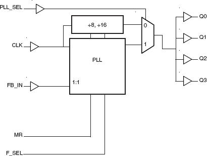
The 86004I is a high performance 1:4 LVCMOS/LVTTL Clock Buffer. The 86004I has a fully integrated PLL and can be configured as zero delay buffer and has an input and output frequency range of 15.625MHz to 62.5MHz. The VCO operates at a frequency range of 250MHz to 500MHz. The external feedback allows the device to achieve "zero delay" between the input clock and the output clocks. The PLL_SEL pin can be used to bypass the PLL for system test and debug purposes. In bypass mode, the reference clock is routed around the PLL and into the internal output divider.
特長
- Four LVCMOS/LVTTL outputs, 7Ω typical output impedance
- Single LVCMOS/LVTTL clock input
- CLK accepts the following input levels: LVCMOS or LVTTL
- Output frequency range: 15.625MHz to 62.5MHz
- Input frequency range: 15.625MHz to 62.5MHz
- VCO range: 250MHz to 500MHz
- External feedback for "zero delay" clock regeneration with configurable frequencies
- Fully integrated PLL
- Cycle-to-cycle jitter: 75ps (maximum)
- Output skew: 65ps (maximum)
- Full 3.3V or 2.5V, or 3.3V core/2.5V output operating supply
- -40°C to 85° ambient operating temperature
- Available in lead-free RoHS compliant package
製品比較
アプリケーション
設計・開発
モデル
ECADモデル
SamacSysの回路図シンボル、PCBフットプリント、および3D CADモデルは、製品オプションテーブルのCADモデルリンクをクリックすることで参照できます。シンボルまたはモデルが対応していない場合は、SamacSysに直接リクエスト可能です。

製品選択
適用されたフィルター