概要
説明
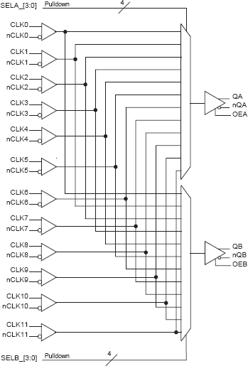
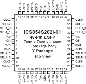
The ICS854S202I-01 is a 12:2 Differential-to-LVDS Clock Multiplexer which can operate up to 3GHz. The ICS854S202I-01 has twelve selectable differential clock inputs, any of which can be independently routed to either of the two LVDS outputs. The CLKx, nCLKx input pairs can accept LVPECL, LVDS or CML levels. The fully differential architecture and low propagation delay make it ideal for use in clock distribution circuits.
特長
- Two differential 2.5V LVDS clock outputs
- Twelve selectable differential clock inputs
- CLKx, nCLKx pairs can accept the following differential input levels: LVPECL, LVDS, CML
- Maximum output frequency: 3GHz
- Propagation delay: 1.1ns (maximum)
- Input skew: 100ps (maximum)
- Output skew: 50ps (maximum)
- Part-to-part skew: 250ps (maximum)
- Additive phase jitter, RMS (12kHz – 20MHz): 0.16ps (typical)
- Full 2.5V operating supply mode
- -40°C to 85°C ambient operating temperature
製品比較
アプリケーション
設計・開発
モデル
ECADモデル
SamacSysの回路図シンボル、PCBフットプリント、および3D CADモデルは、製品オプションテーブルのCADモデルリンクをクリックすることで参照できます。シンボルまたはモデルが対応していない場合は、SamacSysに直接リクエスト可能です。

製品選択
適用されたフィルター