概要
説明
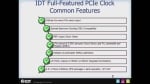
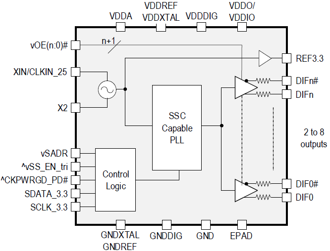
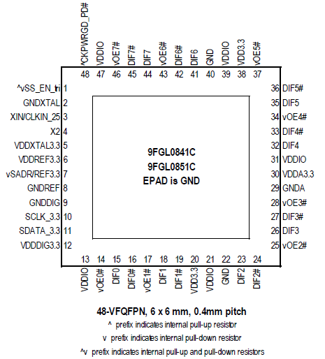
The 9FGL0841/51 devices are 8-output 3.3V PCIe Gen 1–6 clock generators. Each output has a dedicated OE# pin supporting PCIe CLKREQ# functionality. Two different spread spectrum levels, in addition to spread off, are supported. The 9FGL0841/51 supports PCIe Gen 1–6 Common Clocked architectures (CC), PCIe Separate Reference no Spread (SRNS), and Separate Reference Independent Spread (SRIS) clocking architectures.
For information regarding evaluation boards and material, please contact your local sales representative.
特長
- PCIe Gen 1–6 CC-compliant
- Supports PCIe SRIS and SRNS clocking
- Integrated terminations for 100Ω and 85Ω systems save 4 resistors per output
- Pin-selectable SRNS 0%, CC 0%, and CC/SRIS -0.5% spread
- SMBus-selectable CC/SRIS -0.25% spread
- One 3.3V LVCMOS REF output with Wake-On-LAN (WOL) support
- Easy AC coupling to other logic families, see application note AN-891.
- Space-saving 6mm × 6mm 48-VFQFPN
製品比較
アプリケーション
設計・開発
ソフトウェア/ツール
ボード&キット
Evaluation
EVK9FGL0841
アクティブ
Evaluation Board for the 100ohm 9FGL0841 PCIe Clock Generator
This is the evaluation board for the 9FGL0841 clock generator.
Recommended Documents:
モデル
ECADモデル
SamacSysの回路図シンボル、PCBフットプリント、および3D CADモデルは、製品オプションテーブルのCADモデルリンクをクリックすることで参照できます。シンボルまたはモデルが対応していない場合は、SamacSysに直接リクエスト可能です。

製品選択
適用されたフィルター
ビデオ&トレーニング
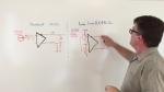
PCIe Reference Clock Jitter Budgets
Ron Wade, chief PCIe system architect explains the fundamental difference in reference clock jitter budgets between the first three generations of the specification and those of Gen4 and Gen5 which raise new challenges for designers.
Related Resources
Video List